TMS320F28027, TMS320F28027-Q1, TMS320F28027F, TMS320F28027F-Q1, TMS320F28026
TMS320F28026-Q1, TMS320F28026F, TMS320F28026F-Q1, TMS320F28023
TMS320F28023-Q1, TMS320F28022, TMS320F28021, TMS320F28020, TMS320F280200
ZHCSA13P –NOVEMBER 2008 –REVISED FEBRUARY 2021
www.ti.com.cn
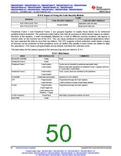
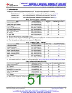
表9-6. Impact of Using the Code Security Module
FLASH
ADDRESS
CODE SECURITY ENABLED
CODE SECURITY DISABLED
0x3F 7F80 to 0x3F 7FEF
0x3F 7FF0 to 0x3F 7FF5
Application code and data
Reserved for data only
Fill with 0x0000
Peripheral Frame 1 and Peripheral Frame 2 are grouped together to enable these blocks to be write/read
peripheral block protected. The protected mode makes sure that all accesses to these blocks happen as written.
Because of the pipeline, a write immediately followed by a read to different memory locations, will appear in
reverse order on the memory bus of the CPU. This can cause problems in certain peripheral applications where
the user expected the write to occur first (as written). The CPU supports a block protection mode where a region
of memory can be protected so that operations occur as written (the penalty is extra cycles are added to align
the operations). This mode is programmable and by default, it protects the selected zones.
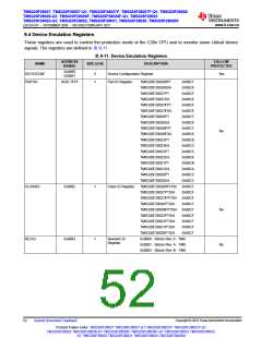
The wait states for the various spaces in the memory map area are listed in 表9-7.
表9-7. Wait States
AREA
M0 and M1 SARAMs
Peripheral Frame 0
Peripheral Frame 1
WAIT STATES (CPU)
0-wait
COMMENTS
Fixed
0-wait
0-wait (writes)
2-wait (reads)
Cycles can be extended by peripheral generated ready.
Back-to-back write operations to Peripheral Frame 1 registers will incur
a 1-cycle stall (1-cycle delay).
Peripheral Frame 2
0-wait (writes)
2-wait (reads)
Fixed. Cycles cannot be extended by the peripheral.
L0 SARAM
OTP
0-wait data and program
Programmable
Assumes no CPU conflicts
Programmed through the Flash registers.
1-wait is minimum number of wait states allowed.
Programmed through the Flash registers.
1-wait minimum
Programmable
FLASH
0-wait Paged min
1-wait Random min
Random ≥Paged
FLASH Password
Boot-ROM
16-wait fixed
0-wait
Wait states of password locations are fixed.
Copyright © 2022 Texas Instruments Incorporated
50
Submit Document Feedback
Product Folder Links: TMS320F28027 TMS320F28027-Q1 TMS320F28027F TMS320F28027F-Q1
TMS320F28026 TMS320F28026-Q1 TMS320F28026F TMS320F28026F-Q1 TMS320F28023 TMS320F28023-
Q1 TMS320F28022 TMS320F28021 TMS320F28020 TMS320F280200

 TI [ TEXAS INSTRUMENTS ]