TMS320F28027, TMS320F28027-Q1, TMS320F28027F, TMS320F28027F-Q1, TMS320F28026
TMS320F28026-Q1, TMS320F28026F, TMS320F28026F-Q1, TMS320F28023
TMS320F28023-Q1, TMS320F28022, TMS320F28021, TMS320F28020, TMS320F280200
ZHCSA13P –NOVEMBER 2008 –REVISED FEBRUARY 2021
www.ti.com.cn
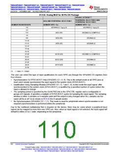
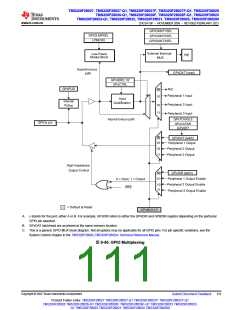
GPIOXINT1SEL
GPIOLMPSEL
LPMCR0
GPIOXINT2SEL
GPIOXINT3SEL
External Interrupt
MUX
Low-Power
Modes Block
PIE
Asynchronous
path
GPxDAT (read)
GPxQSEL1/2
GPxCTRL
GPxPUD
N/C
00
01
Peripheral 1 Input
Peripheral 2 Input
Input
Internal
Pullup
Qualification
10
11
Peripheral 3 Input
GPxTOGGLE
Asynchronous path
GPIOx pin
GPxCLEAR
GPxSET
00
01
GPxDAT (latch)
Peripheral 1 Output
10
11
Peripheral 2 Output
Peripheral 3 Output
High Impedance
Output Control
GPxDIR (latch)
00
01
Peripheral 1 Output Enable
Peripheral 2 Output Enable
0 = Input, 1 = Output
XRS
10
11
Peripheral 3 Output Enable
= Default at Reset
GPxMUX1/2
A. x stands for the port, either A or B. For example, GPxDIR refers to either the GPADIR and GPBDIR register depending on the particular
GPIO pin selected.
B. GPxDAT latch/read are accessed at the same memory location.
C. This is a generic GPIO MUX block diagram. Not all options may be applicable for all GPIO pins. For pin-specific variations, see the
System Control chapter in the TMS320F2802x,TMS320F2802xx Technical Reference Manual.
图9-40. GPIO Multiplexing
Copyright © 2022 Texas Instruments Incorporated
Submit Document Feedback
111
Product Folder Links: TMS320F28027 TMS320F28027-Q1 TMS320F28027F TMS320F28027F-Q1
TMS320F28026 TMS320F28026-Q1 TMS320F28026F TMS320F28026F-Q1 TMS320F28023 TMS320F28023-
Q1 TMS320F28022 TMS320F28021 TMS320F28020 TMS320F280200

 TI [ TEXAS INSTRUMENTS ]