TMS320F28027, TMS320F28027-Q1, TMS320F28027F, TMS320F28027F-Q1, TMS320F28026
TMS320F28026-Q1, TMS320F28026F, TMS320F28026F-Q1, TMS320F28023
TMS320F28023-Q1, TMS320F28022, TMS320F28021, TMS320F28020, TMS320F280200
ZHCSA13P –NOVEMBER 2008 –REVISED FEBRUARY 2021
www.ti.com.cn
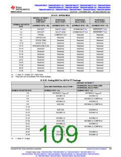
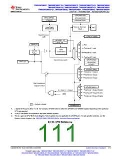
表9-33. Analog MUX for 38-Pin DA Package
DEFAULT AT RESET(1)
PERIPHERAL SELECTION 2 AND
PERIPHERAL SELECTION 3
AIOx AND PERIPHERAL SELECTION 1
AIOMUX1 REGISTER BITS
AIOMUX1 BITS = 0,x
AIOMUX1 BITS = 1,x
1-0
ADCINA0 (I), VREFHI (I)
ADCINA0 (I), VREFHI (I)
3-2
–
–
5-4
AIO2 (I/O)
ADCINA2 (I), COMP1A (I)
7-6
–
–
9-8
AIO4 (I/O)
ADCINA4 (I)
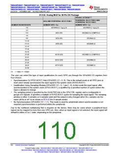
11-10
13-12
15-14
17-16
19-18
21-20
23-22
25-24
27-26
29-28
31-30
–
–
AIO6 (I/O)
ADCINA6 (I)
–
–
–
–
–
–
AIO10 (I/O)
ADCINB2 (I), COMP1B (I)
–
–
AIO12 (I/O)
ADCINB4 (I)
–
–
AIO14 (I/O)
ADCINB6 (I)
–
–
(1) I = Input, O = Output
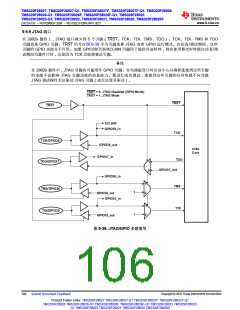
The user can select the type of input qualification for each GPIO pin through the GPxQSEL1/2 registers from
four choices:
• Synchronization To SYSCLKOUT Only (GPxQSEL1/2 = 0, 0): This is the default mode of all GPIO pins at
reset and it simply synchronizes the input signal to the system clock (SYSCLKOUT).
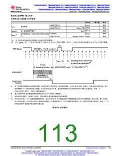
• Qualification Using Sampling Window (GPxQSEL1/2 = 0, 1 and 1, 0): In this mode the input signal, after
synchronization to the system clock (SYSCLKOUT), is qualified by a specified number of cycles before the
input is allowed to change.
• The sampling period is specified by the QUALPRD bits in the GPxCTRL register and is configurable in
groups of 8 signals. It specifies a multiple of SYSCLKOUT cycles for sampling the input signal. The sampling
window is either 3-samples or 6-samples wide and the output is only changed when ALL samples are the
same (all 0s or all 1s) as shown in 图9-42 (for 6 sample mode).
• No Synchronization (GPxQSEL1/2 = 1,1): This mode is used for peripherals where synchronization is not
required (synchronization is performed within the peripheral).
Due to the multilevel multiplexing that is required on the device, there may be cases where a peripheral input
signal can be mapped to more then one GPIO pin. Also, when an input signal is not selected, the input signal will
default to either a 0 or 1 state, depending on the peripheral.
Copyright © 2022 Texas Instruments Incorporated
110
Submit Document Feedback
Product Folder Links: TMS320F28027 TMS320F28027-Q1 TMS320F28027F TMS320F28027F-Q1
TMS320F28026 TMS320F28026-Q1 TMS320F28026F TMS320F28026F-Q1 TMS320F28023 TMS320F28023-
Q1 TMS320F28022 TMS320F28021 TMS320F28020 TMS320F280200

 TI [ TEXAS INSTRUMENTS ]