TMS320C6678
Multicore Fixed and Floating-Point Digital Signal Processor
SPRS691D—April 2013
www.ti.com
3.2 Peripheral Selection After Device Reset
Several of the peripherals on the TMS320C6678 are controlled by the Power Sleep Controller (PSC). By default, the
PCIe, SRIO, and HyperLink are held in reset and clock-gated. The memories in these modules are also in a
low-leakage sleep mode. Software is required to turn these memories on. The software enables the modules (turns
on clocks and de-asserts reset) before these modules can be used.
If one of the above modules is used in the selected ROM boot mode, the ROM code will automatically enable the
module.
All other modules come up enabled by default and there is no special software sequence to enable. For more detailed
information on the PSC usage, see the Power Sleep Controller (PSC) for KeyStone Devices User Guide in ‘‘Related
Documentation from Texas Instruments’’ on page 73.
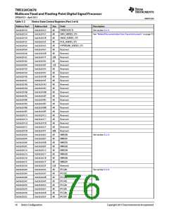
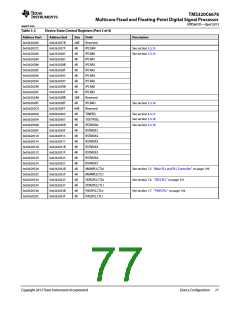
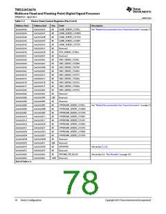
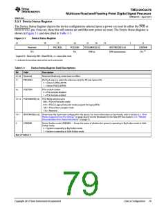
3.3 Device State Control Registers
The TMS320C6678 device has a set of registers that are used to provide the status or configure certain parts of its
peripherals. These registers are shown in Table 3-2.
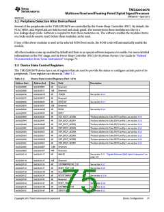
Table 3-2
Device State Control Registers (Part 1 of 4)
Address Start
0x02620000
0x02620008
0x02620018
0x0262001C
0x02620020
0x02620024
0x02620038
0x0262003C
0x02620040
0x02620044
0x02620048
0x0262004C
0x02620050
0x02620054
0x02620058
0x0262005C
0x02620060
0x026200E0
0x02620110
Address End
0x02620007
0x02620017
0x0262001B
0x0262001F
0x02620023
0x02620037
0x0262003B
0x0262003F
0x02620043
0x02620047
0x0262004B
0x0262004F
0x02620053
0x02620057
0x0262005B
0x0262005F
0x026200DF
0x0262010F
0x02620117
Size
8B
16B
4B
Field
Description
Reserved
Reserved
JTAGID
See section 3.3.3
See section 3.3.1
See section 3.3.4
4B
4B
Reserved
DEVSTAT
20B
4B
Reserved
KICK0
4B
4B
4B
4B
4B
4B
4B
4B
4B
KICK1
DSP_BOOT_ADDR0
DSP_BOOT_ADDR1
DSP_BOOT_ADDR2
DSP_BOOT_ADDR3
DSP_BOOT_ADDR4
DSP_BOOT_ADDR5
DSP_BOOT_ADDR6
DSP_BOOT_ADDR7
The boot address for C66x DSP CorePac0, see section 3.3.5
The boot address for C66x DSP CorePac1, see section 3.3.5
The boot address for C66x DSP CorePac2, see section 3.3.5
The boot address for C66x DSP CorePac3, see section 3.3.5
The boot address for C66x DSP CorePac4, see section 3.3.5
The boot address for C66x DSP CorePac5, see section 3.3.5
The boot address for C66x DSP CorePac6, see section 3.3.5
The boot address for C66x DSP CorePac7, see section 3.3.5
128B Reserved
48B
8B
Reserved
MACID
See section 7.21 ‘‘Gigabit Ethernet (GbE) Switch Subsystem’’ on
page 223
0x02620118
0x02620130
0x02620134
0x02620138
0x0262013C
0x02620140
0x02620144
0x02620148
0x0262014C
0x0262012F
0x02620133
0x02620137
0x0262013B
0x0262013F
0x02620143
0x02620147
0x0262014B
0x0262014F
24B
4B
4B
4B
4B
4B
4B
4B
4B
Reserved
LRSTNMIPINSTAT_CLR
RESET_STAT_CLR
Reserved
See section 3.3.7
See section 3.3.9
BOOTCOMPLETE
Reserved
See section 3.3.10
RESET_STAT
See section 3.3.8
See section 3.3.6
See section 3.3.2
LRSTNMIPINSTAT
DEVCFG
Copyright 2013 Texas Instruments Incorporated
Device Configuration 75

 TI [ TEXAS INSTRUMENTS ]