TMS320C6678
Multicore Fixed and Floating-Point Digital Signal Processor
SPRS691D—April 2013
www.ti.com
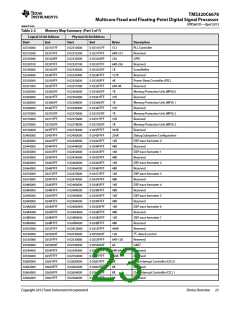
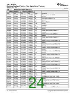
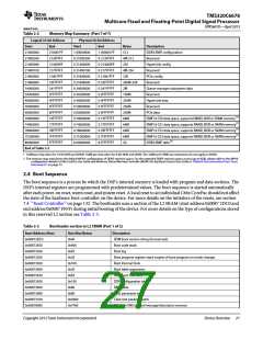
Table 2-2
Memory Map Summary (Part 7 of 7)
Logical 32-bit Address
Physical 36-bit Address
Start
End
Start
End
Bytes
512
Description
21000000
21000200
21400000
21400100
21800000
21808000
34000000
34200000
40000000
50000000
60000000
70000000
74000000
78000000
7C000000
80000000
End of Table 2-2
210001FF
213FFFFF
214000FF
217FFFFF
21807FFF
33FFFFFF
341FFFFF
3FFFFFFF
4FFFFFFF
5FFFFFFF
6FFFFFFF
73FFFFFF
77FFFFFF
7BFFFFFF
7FFFFFFF
FFFFFFFF
1 00000000
0 21000200
0 21400000
0 21400100
0 21800000
0 21808000
0 34000000
0 34200000
0 40000000
0 50000000
0 60000000
0 70000000
0 74000000
0 78000000
0 7C000000
8 00000000
1 000001FF
0 213FFFFF
0 214000FF
0 217FFFFF
0 21807FFF
0 33FFFFFF
0 341FFFFF
0 3FFFFFFF
0 4FFFFFFF
0 5FFFFFFF
0 6FFFFFFF
0 73FFFFFF
0 77FFFFFF
0 7BFFFFFF
0 7FFFFFFF
8 7FFFFFFF
DDR3 EMIF configuration
4M-512
256
Reserved
HyperLink config
4M-256
32K
Reserved
PCIe config
296M-32K
2M
Reserved
Queue manager subsystem data
190M
256M
256M
256M
64M
Reserved
HyperLink data
Reserved
PCIe data
EMIF16 CE0 data space, supports NAND, NOR or SRAM memory(1)
EMIF16 CE1 data space, supports NAND, NOR or SRAM memory(1)
EMIF16 CE2 data space, supports NAND, NOR or SRAM memory(1)
EMIF16 CE3 data space, supports NAND, NOR or SRAM memory(1)
DDR3 EMIF data (2)
64M
64M
64M
2G
1 32MB per chip select for 16-bit NOR and SRAM. 16MB per chip select for 8-bit NOR and SRAM. The 32MB and 16MB size restrictions do not apply to NAND.
2 The memory map only shows the default MPAX configuration of DDR3 memory space. For the extended DDR3 memory space access (up to 8GB), please refer to the MPAX
configuration details in C66x CorePac User Guide and Multicore Shared Memory Controller (MSMC) for KeyStone Devices User Guide in ‘‘Related Documentation from Texas
Instruments’’ on page 73.
2.4 Boot Sequence
The boot sequence is a process by which the DSP's internal memory is loaded with program and data sections. The
DSP's internal registers are programmed with predetermined values. The boot sequence is started automatically
after each power-on reset, warm reset, and system reset. A local reset to an individual C66x CorePac should not affect
the state of the hardware boot controller on the device. For more details on the initiators of the resets, see section
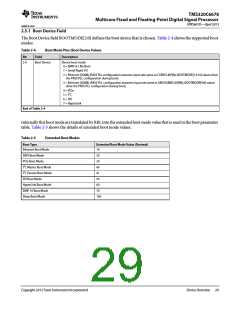
7.4 ‘‘Reset Controller’’ on page 132. The bootloader uses a section of the L2 SRAM (start address 0x0087 2DC0 and
end address 0x0087 FFFF) during initial booting of the device. For more details on the type of configurations stored
in this reserved L2 section see Table 2-3.
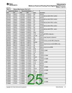
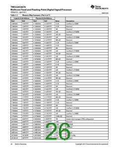
Table 2-3
Bootloader section in L2 SRAM (Part 1 of 2)
Start Address (Hex)
0x00872DC0
0x00872E00
0x00873200
0x008732E0
0x00873300
0x00873400
0x00873420
0x00873500
0x00873600
0x00873680
0x00873700
0x00878000
Size (Hex Bytes)
0x40
Description
ROM boot version string (Unreserved)
Boot code stack
0x400
0xE0
Boot log
0x20
Boot progress register stack (copies of boot program on mode change)
Boot Internal Stats
0x100
0x20
Boot table arguments
0xE0
ROM boot FAR data
0x100
0x80
DDR configuration table
RAM table
0x80
Boot parameter table
0x4900
0x7F80
Clear text packet scratch
Ethernet/SRIO packet/message/descriptor memory
Copyright 2013 Texas Instruments Incorporated
Device Overview 27

 TI [ TEXAS INSTRUMENTS ]