TMS320C6678
Multicore Fixed and Floating-Point Digital Signal Processor
SPRS691D—April 2013
www.ti.com
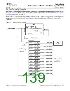
7.5 Main PLL and PLL Controller
This section provides a description of the Main PLL and the PLL Controller. For details on the operation of the PLL
Controller module, see the Phase Locked Loop (PLL) for KeyStone Devices User Guide in ‘‘Related Documentation
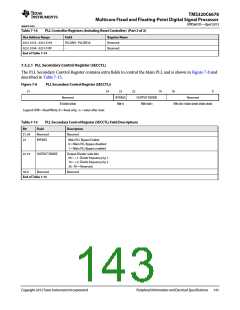
from Texas Instruments’’ on page 73.
The Main PLL is controlled by the standard PLL Controller. The PLL controller manages the clock ratios, alignment,
and gating for the system clocks to the device. Figure 7-7 shows a block diagram of the main PLL and the PLL
Controller.
Figure 7-7
Main PLL and PLL Controller
PLL
PLLD xPLLM /2
CORECLK(N|P)
0
1
PLLOUT
OUTPUT
DIVIDE
BYPASS
PLL Controller
/1
1
0
SYSCLK1
C66x
CorePac
PLLDIV1
/x
/2
/3
/y
1
0
0
PLLDIV2
PLLDIV3
PLLDIV4
PLLDIV5
PLLDIV6
PLLDIV7
PLLDIV8
PLLDIV9
PLLDIV10
PLLDIV11
SYSCLK2
SYSCLK3
SYSCLK4
SYSCLK5
SYSCLK6
SYSCLK7
SYSCLK8
SYSCLK9
SYSCLK10
SYSCLK11
PLLEN
PLLENSRC
/64
/6
To Switch Fabric,
Peripherals,
Accelerators
/z
/12
/3
/6
Copyright 2013 Texas Instruments Incorporated
Peripheral Information and Electrical Specifications 139

 TI [ TEXAS INSTRUMENTS ]