TMS320C6672
Multicore Fixed and Floating-Point Digital Signal Processor
SPRS708C—February 2012
www.ti.com
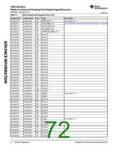
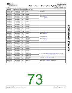
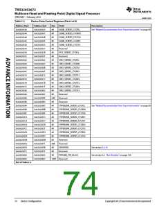
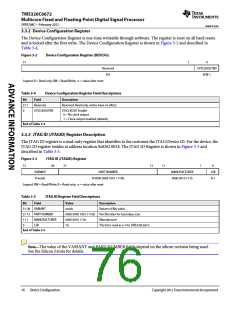
3.3.2 Device Configuration Register
The Device Configuration Register is one-time writeable through software. The register is reset on all hard resets
and is locked after the first write. The Device Configuration Register is shown in Figure 3-2 and described in
Table 3-4.
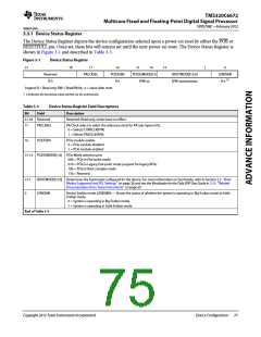
Figure 3-2
Device Configuration Register (DEVCFG)
31
1
0
Reserved
R-0
SYSCLKOUTEN
R/W-1
Legend: R = Read only; RW = Read/Write; -n = value after reset
Table 3-4
Device Configuration Register Field Descriptions
Bit
31-1
0
Field
Description
Reserved
Reserved. Read only, writes have no effect.
SYSCLKOUTEN
SYSCLKOUT Enable
0 = No clock output
1 = Clock output enabled (default)
End of Table 3-4
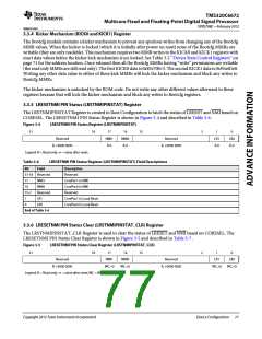
3.3.3 JTAG ID (JTAGID) Register Description
The JTAG ID register is a read-only register that identifies to the customer the JTAG/Device ID. For the device, the
JTAG ID register resides at address location 0x0262 0018. The JTAG ID Register is shown in Figure 3-3 and
described in Table 3-5.
Figure 3-3
JTAG ID (JTAGID) Register
31
28
27
12
11
1
0
VARIANT
R-xxxxb
PART NUMBER
MANUFACTURER
0000 0010 111b
LSB
R-1
R-0000 0000 1001 1110b
Legend: RW = Read/Write; R = Read only; -n = value after reset
Table 3-5
JTAG ID Register Field Descriptions
Bit
Field
Value
Description
Variant (4-Bit) value.
31-28 VARIANT
xxxxb
27-12 PART NUMBER
0000 0000 1001 1110b Part Number for boundary scan
11-1
0
MANUFACTURER
LSB
0000 0010 111b
1b
Manufacturer
This bit is read as a 1 for TMS320C6672
End of Table 3-5
Note—The value of the VARIANT and PART NUMBER fields depend on the silicon revision being used.
See the Silicon Errata for details.
76
Device Configuration
Copyright 2012 Texas Instruments Incorporated

 TI [ TEXAS INSTRUMENTS ]