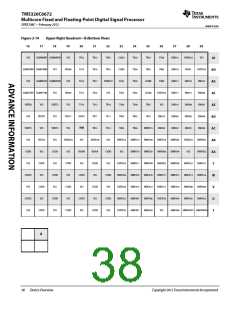
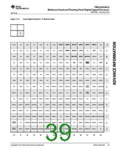
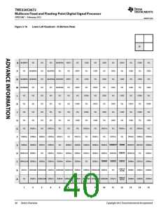
TMS320C6672
Multicore Fixed and Floating-Point Digital Signal Processor
SPRS708C—February 2012
www.ti.com
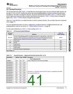
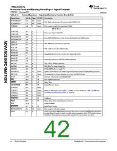
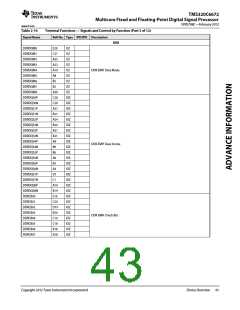
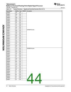
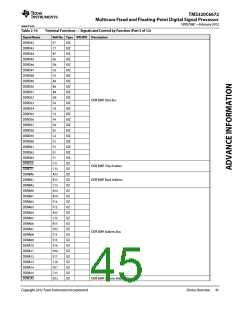
Table 2-16
Terminal Functions — Signals and Control by Function (Part 2 of 12)
Ball No. Type IPD/IPU Description
Signal Name
PCIESSMODE0 †
PCIESSMODE1 †
PCIESSEN †
K24
L27
L24
IOZ
IOZ
I
Down
Down
Down
PCIe Mode selection pins (Pins shared with GPIO[14:15])
PCIe module enable (Pin shared with TIMI0)
Clock / Reset
CORECLKP
CORECLKN
SRIOSGMIICLKP
SRIOSGMIICLKN
DDRCLKP
DDRCLKN
PCIECLKP
PCIECLKN
MCMCLKP
MCMCLKN
PASSCLKP
PASSCLKN
AVDDA1
AG3
AG4
AG6
AJ6
I
Core Clock Input to main PLL.
I
I
RapidIO/SGMII Reference Clock to drive the RapidIO and SGMII SerDes
DDR Reference Clock Input to DDR PLL (
I
G29
H29
AG5
AH5
W2
I
I
I
PCIe Clock Input to drive PCIe SerDes
I
I
HyperLink Reference Clock to drive the HyperLink SerDes
Network Coprocessor (PASS PLL) Reference Clock
Y2
I
AJ5
I
AJ4
I
H22
AC6
AD5
AE3
AE4
AD20
M25
N26
M27
AF2
AD4
AE6
AE5
N25
M29
AC20
N27
AE2
G22
P
SYS_CLK PLL Power Supply Pin
AVDDA2
P
DDR_CLK PLL Power Supply Pin
AVDDA3
P
PASS_CLK PLL Power Supply Pin
SYSCLKOUT
PACLKSEL
HOUT
OZ
Down
Down
UP
System Clock Output to be used as a general purpose output clock for debug purposes
PA clock select to choose between core clock and PASSCLK pins
Interrupt output pulse created by IPCGRH
Non-maskable Interrupt
I
OZ
NMI
I
UP
LRESET
I
UP
Warm Reset
LRESETNMIEN
CORESEL0
CORESEL1
CORESEL2
CORESEL3
RESETFULL
RESET
I
UP
Enable for core selects
I
Down
Down
Down
Down
UP
I
Select for the target core for LRESET and NMI. For more details see Table 7-47‘‘NMI and
Local Reset Timing Requirements’’ on page 177
I
I
I
Full Reset
I
UP
Warm Reset of non isolated portion on the IC
Power-on Reset
POR
I
RESETSTAT
BOOTCOMPLETE
PTV15
O
OZ
A
UP
Reset Status Output
Down
Boot progress indication output
PTV Compensation NMOS Reference Input. A precision resistor placed between the PTV15
pin and ground is used to closely tune the output impedance of the DDR interface drivers
to 50ohms. Presently the recommended value for this 1% resistor is 45.3 ohms.
42
Device Overview
Copyright 2012 Texas Instruments Incorporated

 TI [ TEXAS INSTRUMENTS ]