TMS320C6672
Multicore Fixed and Floating-Point Digital Signal Processor
SPRS708C—February 2012
www.ti.com
6 Device Operating Conditions
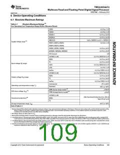
6.1 Absolute Maximum Ratings
Table 6-1
Absolute Maximum Ratings (1)
Over Operating Case Temperature Range (Unless Otherwise Noted)
CVDD
-0.3 V to 1.3 V
-0.3 V to 1.3 V
CVDD1
DVDD15
DVDD18
VREFSSTL
-0.3 V to 2.45 V
-0.3 V to 2.45 V
0.49 × DVDD15 to 0.51 × DVDD15
-0.3 V to 1.3 V
Supply voltage range (2)
:
VDDT1, VDDT2, VDDT3
VDDT4, VDDT5, VDDT6
VDDR1, VDDR2, VDDR3
-0.3 V to 2.45 V
-0.3 V to 2.45 V
0 V
AVDDA1, AVDDA2, AVDDA3
VSS Ground
LVCMOS (1.8V)
DDR3
-0.3 V to DVDD18+0.3 V
-0.3 V to 2.45 V
-0.3 V to 2.45 V
-0.3 V to DVDD18+0.3 V
-0.3 V to 1.3 V
I2C
Input voltage (VI) range:
LVDS
LJCB
SerDes
-0.3 V to CVDD1+0.3 V
-0.3 V to DVDD18+0.3 V
-0.3 V to 2.45 V
-0.3 V to 2.45 V
-0.3 V to CVDD1+0.3 V
0°C to 85°C
LVCMOS (1.8V)
DDR3
I2C
Output voltage (VO) range:
SerDes
Commercial
Extended
Operating case temperature range, TC:
-40°C to 100°C
1000 V
HBM (human body model) (4)
CDM (charged device model) (5)
(3)
ESD stress voltage, VESD
Overshoot/undershoot (6)
:
250 V
LVCMOS (1.8V)
20% Overshoot/Undershoot for 20% of
Signal Duty Cycle
DDR3
I2C
Storage temperature range, Tstg
:
-65°C to 150°C
End of Table 6-1
1 Stresses beyond those listed under "absolute maximum ratings" may cause permanent damage to the device. These are stress ratings only, and functional operation of the
device at these or any other conditions beyond those indicated under "recommended operating conditions" is not implied. Exposure to absolute-maximum-rated
conditions for extended periods may affect device reliability.
2 All voltage values are with respect to VSS
.
3 Electrostatic discharge (ESD) to measure device sensitivity/immunity to damage caused by electrostatic discharges into the device.
4
5
Level listed above is the passing level per ANSI/ESDA/JEDEC JS-001-2010. JEDEC document JEP155 states that 500 V HBM allows safe manufacturing with a standard ESD
control process, and manufacturing with less than 500 V HBM is possible if necessary precautions are taken. Pins listed as 1000 V may actually have higher performance.
Level listed above is the passing level per EIA-JEDEC JESD22-C101E. JEDEC document JEP157 states that 250 V CDM allows safe manufacturing with a standard ESD control
process. Pins listed as 250 V may actually have higher performance.
6 Overshoot/Undershoot percentage relative to I/O operating values - for example the maximum overshoot value for 1.8-V LVCMOS signals is DVDD18 + 0.20 × DVDD18 and
maximum undershoot value would be VSS - 0.20 × DVDD18
Copyright 2012 Texas Instruments Incorporated
Device Operating Conditions
109

 TI [ TEXAS INSTRUMENTS ]