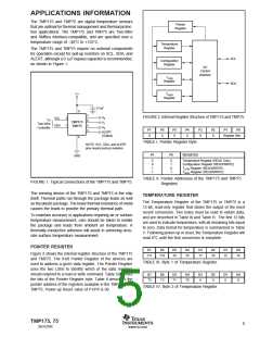
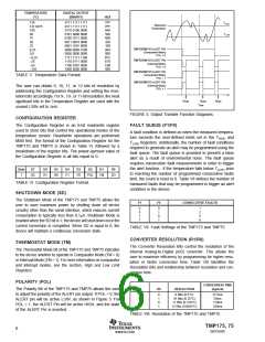
TEMPERATURE
(°C)
DIGITAL OUTPUT
(BINARY)
HEX
128
127.9375
100
80
75
50
25
0.25
0.0
–0.25
–25
–55
–128
0111 1111 1111
0111 1111 1111
0110 0100 0000
0101 0000 0000
0100 1011 0000
0011 0010 0000
0001 1001 0000
0000 0000 0100
0000 0000 0000
1111 1111 1100
1110 0111 0000
1100 1001 0000
1000 0000 0000
7FF
7FF
640
500
4B0
320
190
004
000
FFC
E70
C90
800
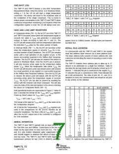
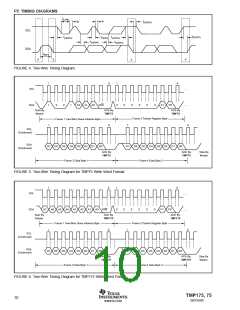
THIGH
Measured
Temperature
TLOW
TMP75/TMP175 ALERT PIN
(Comparator Mode)
POL = 0
TMP75/TMP175 ALERT PIN
(Interrupt Mode)
POL = 0
TMP75/TMP175 ALERT PIN
(Comparator Mode)
POL = 1
TABLE V. Temperature Data Format.
TMP75/TMP175 ALERT PIN
(Interrupt Mode)
POL = 1
The user can obtain 9, 10, 11, or 12 bits of resolution by
addressing the Configuration Register and setting the reso-
lution bits accordingly. For 9-, 10-, or 11-bit resolution, the most
significant bits in the Temperature Register are used with the
unused LSBs set to zero.
Read
Read
Time
Read
FIGURE 3. Output Transfer Function Diagrams.
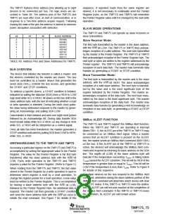
CONFIGURATION REGISTER
The Configuration Register is an 8-bit read/write register
used to store bits that control the operational modes of the
temperature sensor. Read/write operations are performed
MSB first. The format of the Configuration Register for the
TMP175 and TMP75 is shown in Table VI, followed by a
breakdown of the register bits. The power-up/reset value of
the Configuration Register is all bits equal to 0.
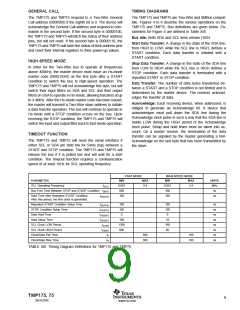
FAULT QUEUE (F1/F0)
A fault condition is defined as when the measured tempera-
ture exceeds the user-defined limits set in the THIGH and
TLOW Registers. Additionally, the number of fault conditions
required to generate an alert may be programmed using the
fault queue. The fault queue is provided to prevent a false
alert as a result of environmental noise. The fault queue
requires consecutive fault measurements in order to trigger
the alert function. If the temperature falls below TLOW, prior
to reaching the number of programmed consecutive faults
limit, the count is reset to 0. Table VII defines the number of
measured faults that may be programmed to trigger an alert
condition in the device.
Byte
D7
D6
D5
D4
D3
D2
D1
D0
1
OS
R1
R0
F1
F0
POL
TM
SD
TABLE VI. Configuration Register Format.
SHUTDOWN MODE (SD)
The Shutdown Mode of the TMP175 and TMP75 allows the
user to save maximum power by shutting down all device
circuitry other than the serial interface, which reduces current
consumption to typically less than 0.1µA. Shutdown Mode is
enabled when the SD bit is 1; the device will shut down once the
current conversion is completed. When SD is equal to 0, the
device will maintain a continuous conversion state.
F1
F0
CONSECUTIVE FAULTS
0
0
1
1
0
1
0
1
1
2
4
6
TABLE VII. Fault Settings of the TMP175 and TMP75.
CONVERTER RESOLUTION (R1/R0)
THERMOSTAT MODE (TM)
The Converter Resolution Bits control the resolution of the
internal Analog-to-Digital (A/D) converter. This allows the
user to maximize efficiency by programming for higher reso-
lution or faster conversion time. Table VIII identifies the
Resolution Bits and relationship between resolution and con-
version time.
The Thermostat Mode bit of the TMP175 and TMP75 indicates
to the device whether to operate in Comparator Mode (TM = 0)
or Interrupt Mode (TM = 1). For more information on comparator
and interrupt modes, see the section, High and Low Limit
Registers.
POLARITY (POL)
CONVERSION TIME
R1
R0
RESOLUTION
(typical)
The Polarity Bit of the TMP175 and TMP75 allows the user
to adjust the polarity of the ALERT pin output. If POL = 0, the
ALERT pin will be active LOW, as shown in Figure 3. For
POL = 1, the ALERT Pin will be active HIGH, and the state
of the ALERT Pin is inverted.
0
0
1
1
0
1
0
1
9 Bits (0.5°C)
10 Bits (0.25°C)
11 Bits (0.125°C)
12 Bits (0.0625°C)
27.5ms
55ms
110ms
220ms
TABLE VIII. Resolution of the TMP175 and TMP75.
TMP175, 75
6
SBOS288C
www.ti.com

 TI [ TEXAS INSTRUMENTS ]