ABSOLUTE MAXIMUM RATINGS(1)
ELECTROSTATIC
DISCHARGE SENSITIVITY
This integrated circuit can be damaged by ESD. Texas
Instruments recommends that all integrated circuits be handled
with appropriate precautions. Failure to observe proper han-
dling and installation procedures can cause damage.
Power Supply, V+ ............................................................................... 7.0V
Input Voltage(2) .................................................................... –0.5V to 7.0V
Input Current ..................................................................................... 10mA
Operating Temperature Range ..................................... –55°C to +127°C
Storage Temperature Range ......................................... –60°C to +130°C
Junction Temperature (TJ Max) .................................................... +150°C
Lead Temperature (soldering) ....................................................... +300°C
NOTES: (1) Stresses above those listed under Absolute Maximum Ratings
may cause permanent damage to the device. Exposure to absolute maximum
conditions for extended periods may affect device reliability. (2) Input voltage
rating applies to all TMP175 and TMP75 input voltages.
ESD damage can range from subtle performance degradation
to complete device failure. Precision integrated circuits may be
more susceptible to damage because very small parametric
changes could cause the device not to meet its published
specifications.
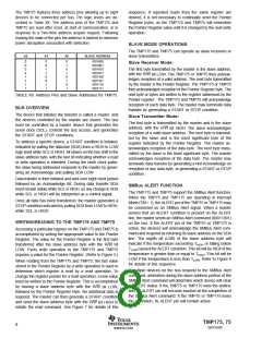
PACKAGE/ORDERING INFORMATION(1)
SPECIFIED
PACKAGE
DESIGNATOR
TEMPERATURE
RANGE
PACKAGE
MARKING
ORDERING
NUMBER
TRANSPORT
MEDIA, QUANTITY
PRODUCT
PACKAGE-LEAD
TMP175
SO-8
D
"
D
"
–40°C to +125°C
TMP175
TMP175AID
TMP175AIDR
TMP75AID
Rails, 100
Tape and Reel, 2500
Rails, 100
"
TMP75
"
"
SO-8
"
"
"
TMP75
"
–40°C to +125°C
"
TMP75AIDR
Tape and Reel, 2500
NOTE: (1) For the most current package and ordering information, see the Package Option Addendum located at the end of this data sheet.
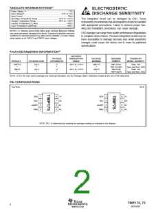
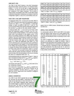
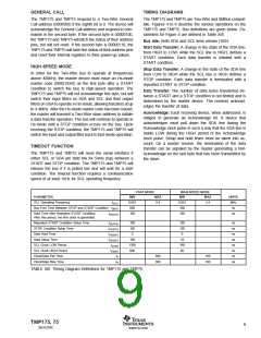
PIN CONFIGURATIONS
Top View
SO-8
1
2
3
4
1
2
3
4
8
7
6
5
SDA
SCL
V+
A0
A1
A2
SDA
SCL
8
7
6
5
V+
A0
A1
A2
ALERT
GND
ALERT
GND
NOTE: Pin 1 is determined by orienting the package marking as indicated in the diagram.
TMP175, 75
2
SBOS288C
www.ti.com

 TI [ TEXAS INSTRUMENTS ]