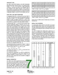
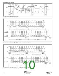
1
9
1
9
…
…
SCL
SDA
1
0
0
1
0
0
0
R/W
0
0
0
0
0
0
P1
P0
Start By
Master
ACK By
TMP175 or TMP75
ACK By
TMP175 or TMP75
Frame 1 Two-Wire Slave Address Byte
Frame 2 Pointer Register Byte
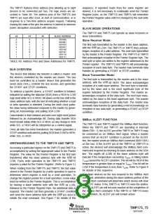
1
9
1
9
SCL
(Continued)
…
SDA
(Continued)
…
0
0
0
1
0
0
1
R/W
D7
D6
D5
D4 D3
D2
D1
D0
Start By
Master
ACK By
TMP175 or TMP75
From
TMP175 or TMP75
ACK By
Master
Frame 3 Two-Wire Slave Address Byte
Frame 4 Data Byte 1 Read Register
1
9
SCL
(Continued)
SDA
(Continued)
D7 D6
D5
D4
D3
D2
D1
D0
From
TMP175 or TMP75
ACK By
Master
Stop By
Master
Frame 5 Data Byte 2 Read Register
NOTE: Address Pins A0, A1, A2 = 0
FIGURE 7. Two-Wire Timing Diagram for Read Word Format.
ALERT
1
0
9
1
9
SCL
SDA
0
0
1
1
0
0
R/W
1
0
0
1
0
0
0
Status
Start By
Master
ACK By
TMP175 or TMP75
From
NACK By Stop By
Master
TMP175 or TMP75 Master
Frame 1 SMBus ALERT Response Address Byte
Frame 2 Slave Address Byte
NOTE: Address Pins A0, A1, A2 = 0
FIGURE 8. Timing Diagram for SMBus ALERT.
TMP175, 75
11
SBOS288C
www.ti.com

 TI [ TEXAS INSTRUMENTS ]