TMP451
SBOS686 –JUNE 2013
www.ti.com
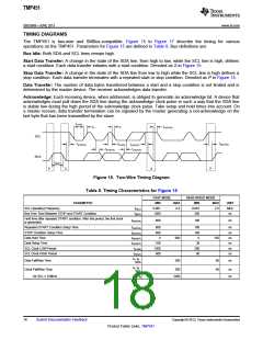
TIMING DIAGRAMS
The TMP451 is two-wire and SMBus-compatible. Figure 15 to Figure 17 describe the timing for various
operations on the TMP451. Parameters for Figure 15 are defined in Table 8. Bus definitions are:
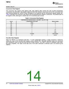
Bus Idle: Both SDA and SCL lines remain high.
Start Data Transfer: A change in the state of the SDA line, from high to low, while the SCL line is high, defines
a start condition. Each data transfer initiates with a start condition. Denoted as S in Figure 15.
Stop Data Transfer: A change in the state of the SDA line from low to high while the SCL line is high defines a
stop condition. Each data transfer terminates with a repeated start or stop condition. Denoted as P in Figure 15.
Data Transfer: The number of data bytes transferred between a start and a stop condition is not limited and is
determined by the master device. The receiver acknowledges data transfer.
Acknowledge: Each receiving device, when addressed, is obliged to generate an acknowledge bit. A device that
acknowledges must pull down the SDA line during the acknowledge clock pulse in such a way that the SDA line
is stable low during the high period of the acknowledge clock pulse. Take setup and hold times into account. On
a master receive, data transfer termination can be signaled by the master generating a not-acknowledge on the
last byte that has been transmitted by the slave.
t(LOW)
tR
tF
t(HDSTA)
SCL
SDA
t(SUSTO)
t(HDSTA)
t(HIGH)
t(SUSTA)
t(SUDAT)
t(HDDAT)
t(BUF)
P
S
S
P
Figure 15. Two-Wire Timing Diagram
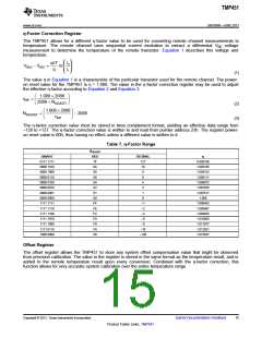
Table 8. Timing Characteristics for Figure 15
FAST MODE
HIGH-SPEED MODE
PARAMETER
MIN
0.001
1300
MAX
MIN
0.001
260
MAX
UNIT
SCL Operating Frequency
f(SCL)
t(BUF)
0.4
2.5
MHz
ns
Bus Free Time Between STOP and START Condition
Hold time after repeated START condition. After this period, the first clock
is generated.
t(HDSTA)
600
160
ns
Repeated START Condition Setup Time
STOP Condition Setup Time
Data Hold Time
t(SUSTA)
t(SUSTO)
t(HDDAT)
t(SUDAT)
t(LOW)
600
600
0
160
160
0
ns
ns
ns
ns
ns
ns
900
300
150
Data Setup Time
100
1300
600
30
SCL Clock LOW Period
SCL Clock HIGH Period
260
60
t(HIGH)
tF, tR
-
Data Fall/Rise Time
80
40
ns
SDA
tF, tR
-
Clock Fall/Rise Time
300
ns
ns
SCL
for SCL ≤ 100kHz
tR
1000
18
Submit Documentation Feedback
Copyright © 2013, Texas Instruments Incorporated
Product Folder Links: TMP451

 TI [ TEXAS INSTRUMENTS ]