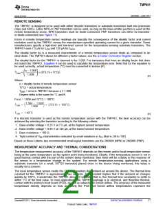
TMP451
www.ti.com
SBOS686 –JUNE 2013
BUS OVERVIEW
The TMP451 is SMBus interface compatible. In SMBus protocol, the device that initiates the transfer is called a
master, and the devices controlled by the master are slaves. The bus must be controlled by a master device that
generates the serial clock (SCL), controls the bus access, and generates the start and stop conditions.
To address a specific device, a start condition is initiated. A start condition is indicated by pulling the data line
(SDA) from a high-to-low logic level while SCL is high. All slaves on the bus shift in the slave address byte, with
the last bit indicating whether a read or write operation is intended. During the ninth clock pulse, the slave being
addressed responds to the master by generating an acknowledge bit and pulling SDA low.
Data transfer is then initiated and sent over eight clock pulses followed by an acknowledge bit. During data
transfer SDA must remain stable while SCL is high, because any change in SDA while SCL is high is interpreted
as a control signal.
After all data have been transferred, the master generates a stop condition. A stop condition is indicated by
pulling SDA from low to high, while SCL is high.
SERIAL INTERFACE
The TMP451 operates only as a slave device on either the two-wire bus or the SMBus. Connections to either bus
are made using the open-drain I/O lines, SDA and SCL. The SDA and SCL pins feature integrated spike
suppression filters and Schmitt triggers to minimize the effects of input spikes and bus noise. The TMP451
supports the transmission protocol for fast (1 kHz to 400 kHz) and high-speed (1 kHz to 2.5 MHz) modes. All
data bytes are transmitted MSB first.
SERIAL BUS ADDRESS
To communicate with the TMP451, the master must first address slave devices using a slave address byte. The
slave address byte consists of seven address bits, and a direction bit indicating the intent of executing a read or
write operation. The TMP451 has a device address of 4Ch (1001 100b). Additional factory-programmed device
addresses are available upon request.
READ/WRITE OPERATIONS
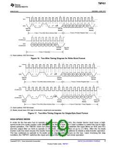
Accessing a particular register on the TMP451 is accomplished by writing the appropriate value to the pointer
register. The value for the pointer register is the first byte transferred after the slave address byte with the R/W
bit low. Every write operation to the TMP451 requires a value for the pointer register (see Figure 16).
When reading from the TMP451, the last value stored in the pointer register by a write operation is used to
determine which register is read by a read operation. To change which register is read for a read operation, a
new value must be written to the pointer register. This transaction is accomplished by issuing a slave address
byte with the R/W bit low, followed by the pointer register byte; no additional data are required. The master can
then generate a start condition and send the slave address byte with the R/W bit high to initiate the read
command; see Figure 17 for details of this sequence.
If repeated reads from the same register are desired, it is not necessary to continually send the pointer register
bytes, because the TMP451 retains the pointer register value until it is changed by the next write operation. Note
that register bytes are sent MSB first, followed by the LSB.
Read operations should be terminated by issuing a not-acknowledge command at the end of the last byte to be
read. For single-byte operation, the master must leave the SDA line high during the acknowledge time of the first
byte that is read from the slave.
Copyright © 2013, Texas Instruments Incorporated
Submit Documentation Feedback
17
Product Folder Links: TMP451

 TI [ TEXAS INSTRUMENTS ]