TMDS361B
SLLS988A –SEPTEMBER 2009–REVISED JULY 2011
www.ti.com
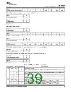
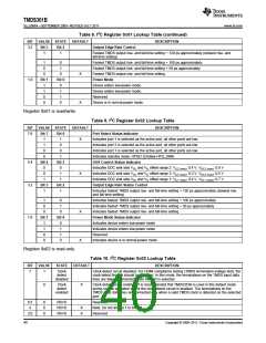
Table 8. I2C Register 0x01 Lookup Table (continued)
BIT
VALUE STATE
DEFAULT
DESCRIPTION
3:2
Bit 3
Bit 2
Output Edge Rate Control
1
1
Fastest TMDS output rise- and fall-time setting + 120 ps approximately (slowest rise- and
fall-time setting)
1
0
Fastest TMDS output rise- and fall-time setting + 100 ps approximately
Fastest TMDS output rise- and fall-time setting + 50 ps approximately
Fastest TMDS output rise- and fall-time setting
Power Mode
0
1
0
Bit 1
1
0
Bit 0
0
X
X
1:0
Device enters low-power mode.
1
1
Device enters low-power mode.
0
1
Reserved
0
0
Device is in normal-power mode.
Register 0x01 is read/write.
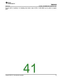
Table 9. I2C Register 0x02 Lookup Table
BIT
VALUE STATE
DEFAULT
DESCRIPTION
Port Select Status Indicator
7:6
Bit 7
Bit 6
1
1
X
Indicates port 1 is selected as the active port, all other ports are low.
Indicates port 2 is selected as the active port, all other ports are low.
Indicates port 3 is selected as the active port, all other ports are low.
Indicates standby mode: HPD[1:3] follow HPD_SINK.
1
0
0
0
0
Bit 4
0
1
Bit 3
0
5:4
3:2
OVS Control Status Indicator
Indicates DDC sink side VOL and VIL offset range 2: VIL2 (max): 0.4 V, VOL2 (max): 0.6 V
Indicates DDC sink side VOL and VIL offset range 3: VIL3 (max): 0.3 V, VOL3 (max): 0.5 V
Indicates DDC sink side VOL and VIL offset range 1: VIL1 (max): 0.4 V, VOL1 (max): 0.7 V
Output Edge Rate Status Control
0
1
X
1
1
Bit 3
1
Bit 2
1
Indicates fastest TMDS output rise- and fall-time setting + 120 ps approximately (slowest rise
and fall time setting)
1
0
Indicates fastest TMDS output rise- and fall-time setting + 100 ps approximately
Indicates fastest TMDS output rise- and fall-time setting + 50 ps approximately
Indicates fastest TMDS output rise- and fall-time setting
Power Mode Status Indicator
0
1
0
Bit 1
1
0
Bit 0
0
X
X
1:0
Indicates device enters low-power mode
1
1
Indicates device enters low-power mode
0
1
Reserved
0
0
Indicates device is in normal-power mode
Register 0x02 is read-only.
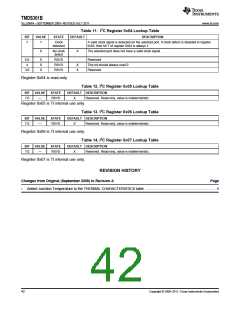
Table 10. I2C Register 0x03 Lookup Table
BIT
VALUE
STATE
DEFAULT
DESCRIPTION
7
1
Clock
detect
disabled
Clock-detect circuit disabled. For HDMI compliance testing (TMDS termination-voltage test), the
clock-detect feature should be disabled. In this mode, the terminations on the TMDS input data
lines are always connected when the port is selected.
0
Clock
detect
enabled
X
Clock-detect circuit enabled. It is recommended that TMDS361B is used in this default mode
during normal operation where the clock detect circuit is enabled. The terminations on the
TMDS input data lines are connected only when a valid TMDS clock is detected on the selected
port.
6:5
4
X
0
0
RSVD
RSVD
RSVD
Reserved
X
X
Note: Do not write a 1 to this bit.
Reserved
3:0
40
Copyright © 2009–2011, Texas Instruments Incorporated

 TI [ TEXAS INSTRUMENTS ]