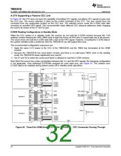
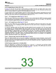
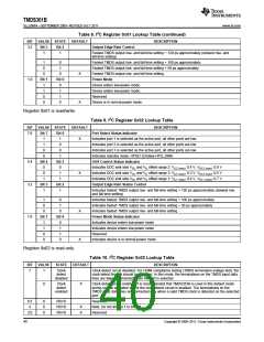
TMDS361B
SLLS988A –SEPTEMBER 2009–REVISED JULY 2011
www.ti.com
Data Output
by Transmitter
Not Acknowledge
Data Output
by Receiver
Acknowledge
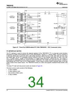
SCL From
1
2
8
9
Master
S
Clock Pulse for
Acknowledgement
START
Condition
T0395-01
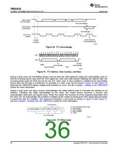
Figure 50. I2C Acknowledge
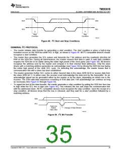
1
2 3 4 5 6 7 8 9 1 2 3 4 5 6 7 8 9
SCL
SDA
Stop
Acknowledge
MSB
Acknowledge
Slave Address
Data
T0396-01
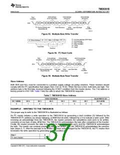
Figure 51. I2C Address, Data Cycle(s), and Stop
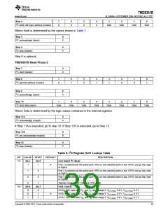
During a write cycle, the transmitting device must not drive the SDA signal line during the acknowledge cycle so
that the receiving device may drive the SDA signal low. After each byte transfer following the address byte, the
receiving device pulls the SDA line low for one SCL clock cycle. A stop condition is initiated by the transmitting
device after the last byte is transferred. An example of a write cycle can be found in Figure 52 and Figure 53.
Note that the TMDS361B allows multiple write transfers to occur. See the Example – Writing to the TMDS361A
section for more information.
During a read cycle, the slave receiver acknowledges the initial address byte if it decodes the address as its
address. Following this initial acknowledge by the slave, the master device becomes a receiver and
acknowledges data bytes sent by the slave. When the master has received all of the requested data bytes from
the slave, the not-acknowledge (A) condition is initiated by the master by keeping the SDA signal high just before
it asserts the stop (P) condition. This sequence terminates a read cycle as shown in Figure 54 and Figure 55.
See the Example – Reading from the TMDS361A section for more information.
From Receiver
A = No Acknowledge (SDA High)
A = Acknowledge
S = Start Condition
P = Stop Condition
W = Write
W
A
Data
A
Data
A
P
S
Slave Address
From Transmitter
R0007-01
Figure 52. I2C Write Cycle
36
Copyright © 2009–2011, Texas Instruments Incorporated

 TI [ TEXAS INSTRUMENTS ]