TMDS361B
www.ti.com
SLLS988A –SEPTEMBER 2009–REVISED JULY 2011
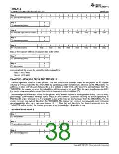
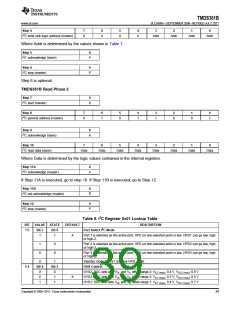
Step 4
7
6
5
4
3
2
1
0
I2C write sink logic address (master)
0
0
0
0
Addr
Addr
Addr
Addr
Where Addr is determined by the values shown in Table 7.
Step 5
8
I2C acknowledge (slave)
A
Step 6
0
I2C stop (master)
P
Step 6 is optional.
TMDS361B Read Phase 2
Step 7
0
I2C start (master)
S
Step 8
7
6
5
4
3
2
1
0
I2C general address (master)
0
1
0
1
1
0
0
1
Step 9
8
I2C acknowledge (slave)
A
Step 10
7
6
5
4
3
2
1
0
I2C read data (slave)
Data
Data
Data
Data
Data
Data
Data
Data
Where Data is determined by the logic values contained in the internal registers.
Step 11A
8
I2C acknowledge (master)
A
If Step 11A is executed, go to step 10. If Step 11B is executed, go to Step 12.
Step 11B
8
I2C not-acknowledge (master)
A
Step 12
0
I2C stop (master)
P
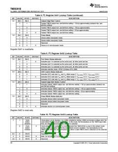
Table 8. I2C Register 0x01 Lookup Table
BIT
VALUE STATE
DEFAULT
DESCRIPTION
7:6
Bit 7
Bit 6
Port Select I2C Mode
1
1
X
Port 1 is selected as the active port; HPD on non-selected ports is low. HPD1 can go low, high
or high-Z.
1
0
0
0
Port 2 is selected as the active port; HPD on non-selected ports is low. HPD2 can go low, high
or high-Z.
Port 3 is selected as the active port; HPD on non-selected ports is low. HPD3 can go low, high
or high-Z.
0
Bit 4
0
1
Bit 3
0
Standby mode: HPD[1:3] follow HPD_SINK.
5:4
OVS Control
OVS2: DDC sink-side VOL and VIL offset range 2: VIL2 (max): 0.4 V, VOL2 (max): 0.6 V
OVS3: DDC sink-side VOL and VIL offset range 3: VIL3 (max): 0.3 V, VOL3 (max): 0.5 V
OVS1: DDC sink-side VOL and VIL offset range 1: VIL1 (max): 0.4 V, VOL1 (max): 0.7 V
0
1
X
1
1
Copyright © 2009–2011, Texas Instruments Incorporated
39

 TI [ TEXAS INSTRUMENTS ]