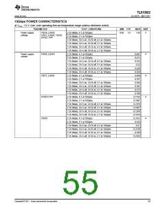
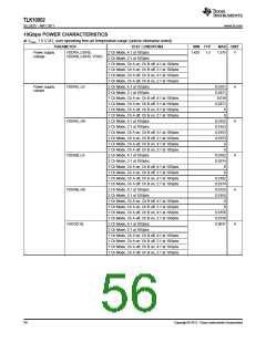
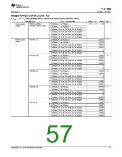
TLK10002
www.ti.com
SLLSE75 –MAY 2011
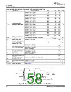
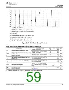
+V0/0
+Vpst
+Vpre
+Vss
0
-Vss
-Vpre
-Vpst
-V0/0
UI
h-1 = TWPRE (0% > -17.5% for typical application) setting
h1 = TWPOST1 (0%
h0 = 1 - |h1| - |h-1|
-37.5% for typical application) setting
>
V0/0 = Output Amplitude with TWPRE = 0%, TWPOST = 0%.
Vss = Steady State Output Voltage = V0/0 * | h1 + h0 + h-1|
Vpre = PreCursor Output Voltage = V0/0 * | -h1 – h0 + h-1|
Vpst = PostCursor Output Voltage = V0/0 * | -h1 + h0 + h-1|
Figure 27. Pre/Post Cursor Swing Definitions
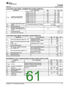
HIGH SPEED SIDE SERIAL RECEIVER CHARACTERISTICS
PARAMETER
TEST CONDITIONS
MIN
50
TYP
MAX UNIT
Full Rate AC Coupled
600
mV
800
VID
RX Input differential voltage |RXP – RXN|
Half/Quarter/Eighth Rate AC Coupled
Full Rate AC Coupled
50
100
100
1200
mVpp
1600
RX Input differential peak-to-peak voltage swing
2 * |RXP – RXN|
VID(pp)
CI
Half/Quarter/Eighth Rate AC Coupled
RX Input capacitance
2
0.66
0.65
0.50
0.35
pF
Zero crossing Half/Quarter/Eighth Rate
Zero crossing Full Rate
Jitter tolerance, total jitter at serial input (DJ +
JTOL
UIpp
RJ) (BER 10-15
)
Zero crossing Half/Quarter/Eighth Rate
Zero crossing Full Rate
JDR
Serial input deterministic jitter (BER 10-15
)
UIpp
100 MHz < f < 0.75*[Serial Bit Rate]
8
dB
dB
SDD11
tskew
Differential input return loss
Intra-pair input skew
0.75 × [Serial Bit Rate] < f < [Serial Bit
Rate]
(1)
See
0.23
UI
UI
t(LATENCY) Receive path latency
See Figure 17
(1) Differential input return loss, SDD11 = 8 – 16.6 log10(f / (0.75 × [Serial Bit Rate])) dB
Copyright © 2011, Texas Instruments Incorporated
59

 TI [ TEXAS INSTRUMENTS ]