TLK10002
SLLSE75 –MAY 2011
www.ti.com
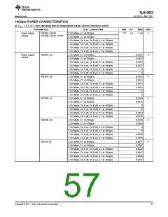
HIGH SPEED SIDE SERIAL TRANSMITTER CHARACTERISTICS
PARAMETER
TEST CONDITIONS
MIN
50
TYP
130
MAX UNIT
220
SWING (3.15:12) = 0000
SWING (3.15:12) = 0001
SWING (3.15:12) = 0010
SWING (3.15:12) = 0011
SWING (3.15:12) = 0100
SWING (3.15:12) = 0101
SWING (3.15:12) = 0110
SWING (3.15:12) = 0111
SWING (3.15:12) = 1000
SWING (3.15:12) = 1001
SWING (3.15:12) = 1010
SWING (3.15:12) = 1011
SWING (3.15:12) = 1100
SWING (3.15:12) = 1101
SWING (3.15:12) = 1110
SWING (3.15:12) = 1111
110
180
250
320
390
460
530
590
660
740
820
890
970
1060
1090
220
320
300
430
390
540
480
650
570
770
660
880
750
1000
mVpp
1100
TX Output differential
peak-to-peak voltage swing
VOD(pp)
830
930
1220
1320
1430
1520
1610
1680
1740
1020
1110
1180
1270
1340
1400
TX Output common mode
voltage
VDDT
-
VCMT
tskew
tr, tf
100-Ω differential termination, DC-coupled
mV
(0.25*VOD(pp)
)
Intra-pair output skew
SWING(3.15:12) = 0110
0.09
UI
ps
Differential output signal rise,
Fall time (20% to 80%)
20
Differential load = 100Ω
Serial Rate ≤ 3.072 Gbps
(Not Applicable to LV-II)
0.35
0.30
0.17
0.15
0.279
0.14
Serial output total jitter (CPRI
LV/LV-II and OBSAI Rates)
JT1
UI
UI
UI
Serial Rate > 3.072 Gbps
(And All LV-II Rates)
Serial Rate ≤ 3.072 Gbps
(Not Applicable to LV-II)
Serial output deterministic
jitter (CPRI LV/LV-II and
OBSAI Rates)
JD1
Serial Rate > 3.072 Gbps
(And All LV-II Rates)
Serial output total jitter (CPRI
E.6/12.HV)
JT2
JD2
CPRI E.6/12.HV (0.6144 and 1.2288 Gbps)
Serial output deterministic
jitter (CPRI E.6/12.HV)
100MHz < f < 1.0 GHz
1.0GHz < f < 5.0 GHz
See Figure 17
7
5
Common-mode output return
loss
Scc22
dB
UI
T(LATENCY) Transmit path latency
0.5 * VDE
VOD(pp)
*
0.5 *
VOD(pp)
VCMT
0.25 * VDE * VOD(pp)
0.25 * VOD(pp)
tr , tf
bit
time
Figure 26. Transmit Output Waveform Parameter Definitions
58
Copyright © 2011, Texas Instruments Incorporated

 TI [ TEXAS INSTRUMENTS ]