TLC7528C, TLC7528E, TLC7528I
DUAL 8-BIT MULTIPLYING
DIGITAL-TO-ANALOG CONVERTERS
SLAS062B – JANUARY 1987 – REVISED MARCH 2000
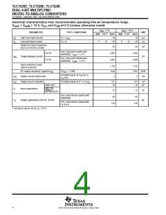
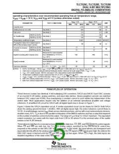
operating characteristics over recommended operating free-air temperature range,
V
= V
= 10 V, V
and V
at 0 V (unless otherwise noted)
refA
refB
OA
OB
V
= 5 V
DD
TYP
V
= 15 V
DD
PARAMETER
TEST CONDITIONS
UNIT
MIN
MAX
±1/2
100
MIN
TYP
MAX
±1/2
100
2.5
Linearity error
LSB
ns
Settling time (to 1/2 LSB)
Gain error
See Note 1
See Note 2
2.5
LSB
REFA to OUTA
REFB to OUTB
–65
–65
0.007
–65
–65
AC feedthrough
See Note 3
dB
Temperature coefficient of gain
See Note 4
See Note 5
0.0035 %FSR/°C
Propagation delay (from digital input to
90% of final analog output current)
80
80
ns
REFA to OUTB See Note 6
REFB to OUTA See Note 7
77
77
77
77
Channel-to-channel
isolation
dB
Measured for code transition
from 00000000 to 11111111,
= 25°C
Digital-to-analog glitch impulse area
Digital crosstalk
160
440
nV•s
T
A
Measured for code transition
from 00000000 to 11111111,
30
60
nV•s
T
A
= 25°C
Harmonic distortion
V = 6 V, f = 1 kHz,
i
T
A
= 25°C
–85
–85
dB
NOTES: 1. OUTA, OUTB load = 100 Ω, C
= 13 pF; WR and CS at 0 V; DB0–DB7 at 0 V to V
or V
to 0 V.
DD
ref
ext
DD
2. Gain error is measured using an internal feedback resistor. Nominal full scale range (FSR) = V – 1 LSB.
3.
4. Temperature coefficient of gain measured from 0°C to 25°C or from 25°C to 70°C.
5. = V = 10 V; OUTA/OUTB load = 100 Ω, C = 13 pF; WR and CS at 0 V; DB0–DB7 at 0 V to V
V
ref
= 20 V peak-to-peak, 100-kHz sine wave; DAC data latches loaded with 00000000.
V
refA
or V to 0 V.
DD
refB ext
DD
= 0; T = 25°C.
6. Both DAC latches loaded with 11111111; V
7. Both DAC latches loaded with 11111111; V
= 20 V peak-to-peak, 100-kHz sine wave; V
= 20 V peak-to-peak, 100-kHz sine wave; V
refA
refB
refB
refA
A
= 0; T = 25°C.
A
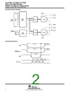
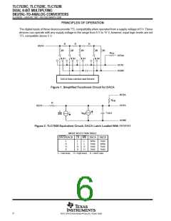
PRINCIPLES OF OPERATION
These devices contain two identical, 8-bit-multiplying D/A converters, DACA and DACB. Each DAC consists
of an inverted R-2R ladder, analog switches, and input data latches. Binary-weighted currents are switched
between DAC output and AGND, thus maintaining a constant current in each ladder leg independent of the
switch state. Most applications require only the addition of an external operational amplifier and voltage
reference. A simplified D/A circuit for DACA with all digital inputs low is shown in Figure 1.
Figure 2 shows the DACA equivalent circuit. A similar equivalent circuit can be drawn for DACB. Both DACs
share the analog ground terminal 1 (AGND). With all digital inputs high, the entire reference current flows to
OUTA. A small leakage current (I ) flows across internal junctions, and as with most semiconductor devices,
Ikg
doubles every 10°C. C is due to the parallel combination of the NMOS switches and has a value that depends
o
onthenumberofswitchesconnectedtotheoutput. TherangeofC is50pFto120pFmaximum. Theequivalent
o
output resistance (r ) varies with the input code from 0.8R to 3R where R is the nominal value of the ladder
o
resistor in the R-2R network.
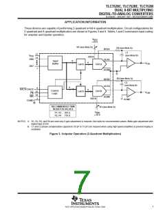
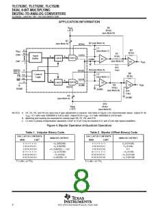
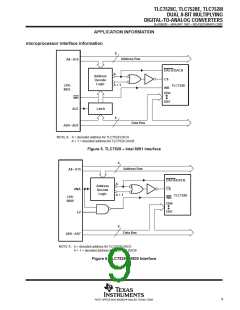
These devices interface to a microprocessor through the data bus, CS, WR, and DACA/DACB control signals.
When CS and WR are both low, the TLC7528 analog output, specified by the DACA/DACB control line,
responds to the activity on the DB0–DB7 data bus inputs. In this mode, the input latches are transparent and
input data directly affects the analog output. When either the CS signal or WR signal goes high, the data on the
DB0–DB7 inputs is latched until the CS and WR signals go low again. When CS is high, the data inputs are
disabled regardless of the state of the WR signal.
5
POST OFFICE BOX 655303 • DALLAS, TEXAS 75265

 TI [ TEXAS INSTRUMENTS ]