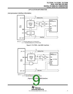
TLC7528C, TLC7528E, TLC7528I
DUAL 8-BIT MULTIPLYING
DIGITAL-TO-ANALOG CONVERTERS
SLAS062B – JANUARY 1987 – REVISED MARCH 2000
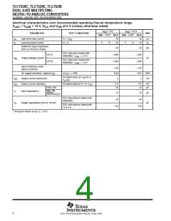
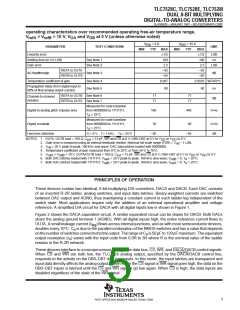
electrical characteristics over recommended operating free-air temperature range,
V
= V
= 10 V, V
and V
at 0 V (unless otherwise noted)
refA
refB
OA
OB
V
= 5 V
V
= 15 V
DD
DD
MIN TYP
PARAMETER
TEST CONDITIONS
V = V
UNIT
†
†
MIN TYP
MAX
10
MAX
10
I
I
High-level input current
Low-level input current
µA
µA
IH
I
DD
V = 0
I
5
12
–10
5
12
–10
IL
Reference input impedance
REFA or REFB to AGND
20
±400
±400
20
±200
±200
kΩ
DAC data latch loaded with
00000000, V = ±10 V
OUTA
OUTB
refA
DAC data latch loaded with
00000000, V = ±10 V
I
Output leakage current
nA
Ikg
refB
Input resistance match
(REFA to REFB)
±1%
0.04
2
±1%
0.02
2
DC supply sensitivity, ∆gain/∆V
Supply current (quiescent)
Supply current (standby)
∆V
DD
= ±10%
%/%
mA
DD
All digital inputs at V min or
IH
I
I
DD
V max
IL
All digital inputs at 0 V or V
0.5
10
0.5
10
mA
pF
DD
DD
DB0–DB7
C
C
Input capacitance
WR, CS,
DACA/DACB
i
15
50
15
50
pF
DAC data latches loaded with
00000000
Output capacitance (OUTA, OUTB)
pF
o
DAC data latches loaded with
11111111
120
120
†
All typical values are at T = 25°C.
A
4
POST OFFICE BOX 655303 • DALLAS, TEXAS 75265

 TI [ TEXAS INSTRUMENTS ]