TL284x, TL384x
CURRENT-MODE PWM CONTROLLERS
SLVS038E – JANUARY 1989 – REVISED DECEMBER 1999
APPLICATION INFORMATION
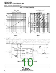
TIMING RESISTANCE
vs
DEAD TIME
vs
FREQUENCY
TIMING CAPACITANCE
100
40
100
40
C
= 10 nF
V
R
T
A
= 15 V
≥ 5 kΩ
= 25°C
T
CC
T
C = 4.7 nF
T
C
= 22 nF
T
C
= 1 nF
T
10
4
C
= 22 nF
T
10
4
C
= 47 nF
T
1
C
= 100 nF
T
0.4
V
T
A
= 15 V
CC
= 25°C
1
100
0.1
1 k
10 k
100 k
1 M
0
4
10
40
100
f - Frequency - Hz
C
– Timing Capacitance – nF
T
Figure 4
Figure 5
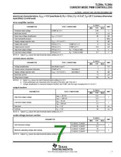
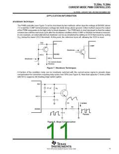
open-loop laboratory test fixture
In the open-loop laboratory test fixture shown in Figure 6, high peak currents associated with loads necessitate
careful grounding techniques. Timing and bypass capacitors should be connected close to the GND terminal
in a single-point ground. The transistor and 5-kΩ potentiometer sample the oscillator waveform and apply an
adjustable ramp to the ISENSE terminal.
REF
R
T
A
V
CC
4.7 kΩ
2N2222
DUT
REF
100 kΩ
COMP
VFB
0.1 µF
1 kΩ
Error Amplifier
Adjust
V
CC
TL284x
TL384x
0.1 µF
1 kΩ, 1 W
ISENSE
RT/CT
OUTPUT
5 kΩ
OUTPUT
GND
4.7 kΩ
ISENSE
Adjust
GND
C
T
Figure 6. Open-Loop Laboratory Test Fixture
10
POST OFFICE BOX 655303 • DALLAS, TEXAS 75265

 TI [ TEXAS INSTRUMENTS ]