THS4531
www.ti.com
SLOS358B –SEPTEMBER 2011–REVISED MARCH 2012
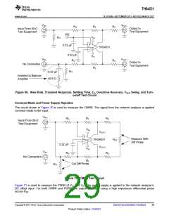
VIN+
VOUT–
RG
RF
RO
Output to
Test Equipment
Input From 50-Ω
Test Equipment
PD
RIT
VS+
+
VOCM
0.22 μF
THS4531
–
0.22 μF
VS–
VIN–
VOUT+
RG
RO
Output to
Test Equipment
No Connection
RF
RIT
0.22 μF
49.9 Ω
Installed to Balance
Amplifier
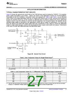
Figure 69. Slew Rate, Transient Response, Settling Time, ZO, Overdrive Recovery, VOUT Swing, and Turn-
on/off Test Circuit
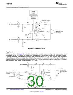
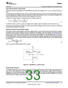
Common-Mode and Power Supply Rejection
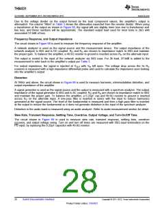
The circuit shown in Figure 70 is used to measure the CMRR. The signal from the network analyzer is applied
common-mode to the input.
VIN+
RG
RF
RO
Input From 50-Ω
Test Equipment
VS+
VOUT–
THS4531
VOUT+
+
VOCM
Measure With
Diff Probe
ROT
–
0.22 μF
VS–
VIN–
RG
RO
No Connection
RF
Cal Diff Probe
RIT
Figure 70. CMRR Test Circuit
Figure 71 is used to measure the PSRR of VS+ and VS-. The power supply is applied to the network analyzer’s
DC offset input. For both CMRR and PSRR, the output is probed using a high impedance differential probe
across ROT
.
Copyright © 2011–2012, Texas Instruments Incorporated
Submit Documentation Feedback
29
Product Folder Link(s): THS4531

 TI [ TEXAS INSTRUMENTS ]