TCA6424A
SCPS193B –JULY 2010–REVISED SEPTEMBER 2010
www.ti.com
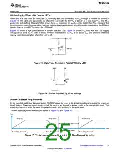
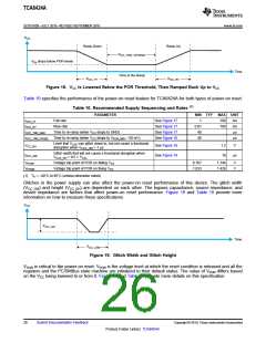
V
CC
Ramp-Down
Ramp-Up
V
CC_TRR_VPOR50
V
drops below POR levels
IN
Time
Time to Re-Ramp
V
V
CC_FT
CC_RT
Figure 18. VCC is Lowered Below the POR Threshold, Then Ramped Back Up to VCC
Table 10 specifies the performance of the power-on reset feature for TCA6424A for both types of power-on reset.
(1)
Table 10. Recommended Supply Sequencing and Rates
PARAMETER
MIN TYP
MAX UNIT
tVCC_FT
Fall rate
See Figure 17
See Figure 17
See Figure 17
See Figure 18
1
0.01
40
100
100
ms
ms
ms
tVCC_RT
Rise rate
tVCC_TRR_GND
tVCC_TRR_POR50
Time to re-ramp (when VCC drops to GND)
Time to re-ramp (when VCC drops to VPOR_MIN – 50 mV)
40
ms
Level that VCCP can glitch down to, but not cause a functional
disruption when VCCX_GW = 1 ms
VCC_GH
tVCC_GW
See Figure 19
See Figure 19
1.2
10
V
Glitch width that will not cause a functional disruption when
VCCX_GH = 0.5 × VCCx
ms
VPORF
VPORR
Voltage trip point of POR on falling VCC
Voltage trip point of POR on fising VCC
0.767
1.033
1.144
1.428
V
V
(1) TA = –40°C to 85°C (unless otherwise noted)
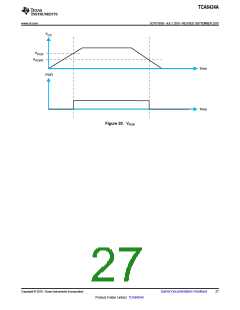
Glitches in the power supply can also affect the power-on reset performance of this device. The glitch width
(VCC_GW) and height (VCC_GH) are dependent on each other. The bypass capacitance, source impedance, and
device impedance are factors that affect power-on reset performance. Figure 19 and Table 10 provide more
information on how to measure these specifications.
V
CC
V
CC_GH
Time
V
CC_GW
Figure 19. Glitch Width and Glitch Height
VPOR is critical to the power-on reset. VPOR is the voltage level at which the reset condition is released and all the
registers and the I2C/SMBus state machine are initialized to their default states. The value of VPOR differs based
on the VCC being lowered to or from 0. Figure 20 and Table 10 provide more details on this specification.
26
Submit Documentation Feedback
Copyright © 2010, Texas Instruments Incorporated
Product Folder Link(s): TCA6424A

 TI [ TEXAS INSTRUMENTS ]