TAS5711
SLOS600 –DECEMBER 2009
www.ti.com
During multiple-byte read operations, the DAP responds with data, a byte at a time, starting at the subaddress
assigned, as long as the master device continues to respond with acknowledges. If a particular subaddress does
not contain 32 bits, the unused bits are read as logic 0.
During multiple-byte write operations, the DAP compares the number of bytes transmitted to the number of bytes
that are required for each specific subaddress. For example, if a write command is received for a biquad
subaddress, the DAP expects to receive five 32-bit words. If fewer than five 32-bit data words have been
received when a stop command (or another start command) is received, the data received is discarded.
Supplying a subaddress for each subaddress transaction is referred to as random I2C addressing. The TAS5711
also supports sequential I2C addressing. For write transactions, if a subaddress is issued followed by data for
that subaddress and the 15 subaddresses that follow, a sequential I2C write transaction has taken place, and the
data for all 16 subaddresses is successfully received by the TAS5711. For I2C sequential write transactions, the
subaddress then serves as the start address, and the amount of data subsequently transmitted, before a stop or
start is transmitted, determines how many subaddresses are written. As was true for random addressing,
sequential addressing requires that a complete set of data be transmitted. If only a partial set of data is written to
the last subaddress, the data for the last subaddress is discarded. However, all other data written is accepted;
only the incomplete data is discarded.
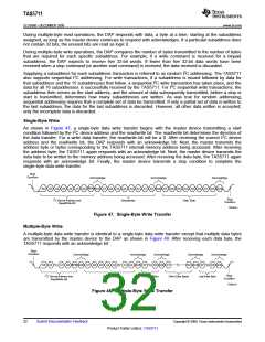
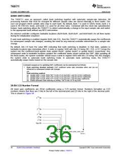
Single-Byte Write
As shown in Figure 47, a single-byte data write transfer begins with the master device transmitting a start
condition followed by the I2C device address and the read/write bit. The read/write bit determines the direction of
the data transfer. For a write data transfer, the read/write bit will be a 0. After receiving the correct I2C device
address and the read/write bit, the DAP responds with an acknowledge bit. Next, the master transmits the
address byte or bytes corresponding to the TAS5711 internal memory address being accessed. After receiving
the address byte, the TAS5711 again responds with an acknowledge bit. Next, the master device transmits the
data byte to be written to the memory address being accessed. After receiving the data byte, the TAS5711 again
responds with an acknowledge bit. Finally, the master device transmits a stop condition to complete the
single-byte data write transfer.
Start
Condition
Acknowledge
Acknowledge
Acknowledge
R/W
A6 A5 A4 A3 A2 A1 A0
ACK A7 A6 A5 A4 A3 A2 A1 A0 ACK D7 D6 D5 D4 D3 D2 D1 D0 ACK
I2C Device Address and
Read/Write Bit
Subaddress
Data Byte
Stop
Condition
T0036-01
Figure 47. Single-Byte Write Transfer
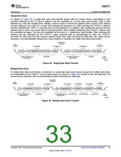
Multiple-Byte Write
A multiple-byte data write transfer is identical to a single-byte data write transfer except that multiple data bytes
are transmitted by the master device to the DAP as shown in Figure 48. After receiving each data byte, the
TAS5711 responds with an acknowledge bit.
Start
Condition
Acknowledge
Acknowledge
Acknowledge
D0 ACK D7
Acknowledge
D0 ACK D7
Acknowledge
D0 ACK
A6 A5
A1 A0 R/W ACK A7 A6 A5 A4 A3
A1 A0 ACK D7
I2C Device Address and
Read/Write Bit
Subaddress
First Data Byte
Last Data Byte
Stop
Condition
Other Data Bytes
T0036-02
Figure 48. Multiple-Byte Write Transfer
32
Submit Documentation Feedback
Copyright © 2009, Texas Instruments Incorporated
Product Folder Link(s): TAS5711

 TI [ TEXAS INSTRUMENTS ]