TAS5711
www.ti.com
SLOS600 –DECEMBER 2009
SSTIMER FUNCTIONALITY
The SSTIMER pin uses a capacitor connected between this pin and ground to control the output duty cycle when
exiting all-channel shutdown. The capacitor on the SSTIMER pin is slowly charged through an internal current
source, and the charge time determines the rate at which the output transitions from a near zero duty cycle to the
desired duty cycle. This allows for a smooth transition that minimizes audible pops and clicks. When the part is
shutdown the drivers are tristated and transition slowly down through a 3K resistor, similarly minimizing pops and
clicks. The shutdown transition time is independent of SSTIMER pin capacitance. Larger capacitors will increase
the start-up time, while capacitors smaller than 2.2 nF will decrease the start-up time. The SSTIMER pin should
be left floating for BD modulation (BTL and PBTL modes) and in 2.1 mode.
CLOCK, AUTO DETECTION, AND PLL
The TAS5711 is a slave device. It accepts MCLK, SCLK, and LRCLK. The digital audio processor (DAP)
supports all the sample rates and MCLK rates that are defined in the clock control register .
The TAS5711 checks to verify that SCLK is a specific value of 32 fS, 48 fS, or 64 fS. The DAP only supports a 1 ×
fS LRCLK. The timing relationship of these clocks to SDIN is shown in subsequent sections. The clock section
uses MCLK or the internal oscillator clock (when MCLK is unstable, out of range, or absent) to produce the
internal clock (DCLK) running at 512 time the PWM switching frequency.
The DAP can autodetect and set the internal clock control logic to the appropriate settings for all supported clock
rates as defined in the clock control register.
TAS5711 has robust clock error handling that uses the bulit-in trimmed oscillator clock to quickly detect
changes/errors. Once the system detects a clock change/error, it will mute the audio (through a single step mute)
and then force PLL to limp using the internal oscillator as a reference clock. Once the clocks are stable, the
system will auto detect the new rate and revert to normal operation. During this process, the default volume will
be restored in a single step (also called hard unmute). The ramp process can be programmed to ramp back
slowly (also called soft unmute) as defined in volume register (0x0E).
SERIAL DATA INTERFACE
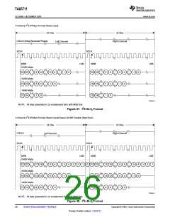
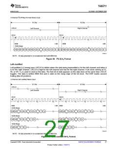
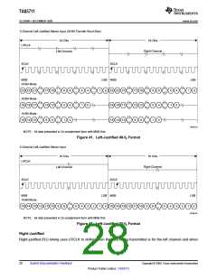
Serial data is input on SDIN. The PWM outputs are derived from SDIN. The TAS5711 DAP accepts serial data in
16-, 20-, or 24-bit left-justified, right-justified, and I2S serial data formats.
PWM Section
The TAS5711 DAP device uses noise-shaping and sophisticated non-linear correction algorithms to achieve high
power efficiency and high-performance digital audio reproduction. The DAP uses a fourth-order noise shaper to
increase dynamic range and SNR in the audio band. The PWM section accepts 24-bit PCM data from the DAP
and outputs two BTL PWM audio output channels.
The PWM section has individual channel dc blocking filters that can be enabled and disabled. The filter cutoff
frequency is less than 1 Hz. Individual channel de-emphasis filters for 44.1- and 48-kHz are included and can be
enabled and disabled.
Finally, the PWM section has an adjustable maximum modulation limit of 93.8% to 99.2%.
For detailed description of using audio processing features like DRC, EQ, 3D, and Bass Boost, please refer to
User's Guide and TAS570X GDE software development tool documentation. Also refer to GDE software
development tool for device data path.
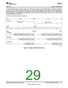
SERIAL INTERFACE CONTROL AND TIMING
The I2S mode is set by writing to register 0x04.
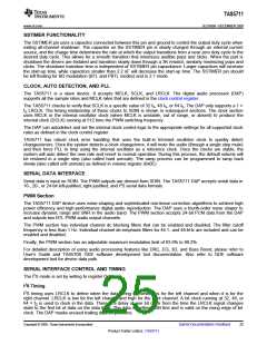
I2S Timing
I2S timing uses LRCLK to define when the data being transmitted is for the left channel and when it is for the
right channel. LRCLK is low for the left channel and high for the right channel. A bit clock running at 32, 48, or
64 × fS is used to clock in the data. There is a delay of one bit clock from the time the LRCLK signal changes
state to the first bit of data on the data lines. The data is written MSB first and is valid on the rising edge of bit
clock. The DAP masks unused trailing data bit positions.
Copyright © 2009, Texas Instruments Incorporated
Submit Documentation Feedback
25
Product Folder Link(s): TAS5711

 TI [ TEXAS INSTRUMENTS ]