TAS5711
www.ti.com
SLOS600 –DECEMBER 2009
DETAILED DESCRIPTION
POWER SUPPLY
To facilitate system design, the TAS5711 needs only a 3.3-V supply in addition to the (typical) 18-V power-stage
supply. An internal voltage regulator provides suitable voltage levels for the gate drive circuitry. Additionally, all
circuitry requiring a floating voltage supply, e.g., the high-side gate drive, is accommodated by built-in bootstrap
circuitry requiring only a few external capacitors.
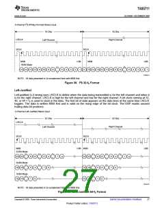
In order to provide good electrical and acoustical characteristics, the PWM signal path for the output stage is
designed as identical, independent half-bridges. For this reason, each half-bridge has separate bootstrap pins
(BST_x), and power-stage supply pins (PVDD_x). The gate drive voltages (GVDD_AB and GVDD_CD) are
derived from the PVDD voltage. Special attention should be paid to placing all decoupling capacitors as close to
their associated pins as possible. In general, inductance between the power-supply pins and decoupling
capacitors must be avoided.
For a properly functioning bootstrap circuit, a small ceramic capacitor must be connected from each bootstrap pin
(BST_x) to the power-stage output pin (OUT_x). When the power-stage output is low, the bootstrap capacitor is
charged through an internal diode connected between the gate-drive regulator output pin (GVDD_x) and the
bootstrap pin. When the power-stage output is high, the bootstrap capacitor potential is shifted above the output
potential and thus provides a suitable voltage supply for the high-side gate driver. In an application with PWM
switching frequencies in the range from 352 kHz to 384 kHz, it is recommended to use 33-nF 50-V X7R
capacitors, size 0603 or 0805, for the bootstrap supply. These 33-nF capacitors ensure sufficient energy storage,
even during minimal PWM duty cycles, to keep the high-side power stage FET (LDMOS) fully turned on during
the remaining part of the PWM cycle.
Special attention should be paid to the power-stage power supply; this includes component selection, PCB
placement, and routing. As indicated, each half-bridge has independent power-stage supply pins (PVDD_x). For
optimal electrical performance, EMC compliance, and system reliability, it is important that each PVDD_x pin is
decoupled with a 100-nF ceramic capacitor placed as close as possible to each supply pin.
The TAS5711 is fully protected against erroneous power-stage turnon due to parasitic gate charging.
ERROR REPORTING
The A_SEL pin has two functions: I2C device-address select and fault indication. On RESET, this pin is an input
and defines the I2C address. But this pin can be programmed after RESET to be an output by writing 1 to bit 0 of
I2C register 0x05. In that mode, the A_SEL pin has the definition shown in Table 1.
Any fault resulting in device shutdown is signaled by the A_SEL pin going low (see Table 1). A latched version of
this pin is available on D1 of register 0x02. The bit can be cleared only by an I2C write.
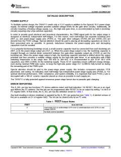
Table 1. FAULT Output States
FAULT
DESCRIPTION
0
Overcurrent (OC) or undervoltage (UVP) error or overtemperature error (OTE) or over
voltage ERROR
1
No faults (normal operation)
Copyright © 2009, Texas Instruments Incorporated
Submit Documentation Feedback
23
Product Folder Link(s): TAS5711

 TI [ TEXAS INSTRUMENTS ]