TAS5715
www.ti.com
SLOS645 –AUGUST 2010
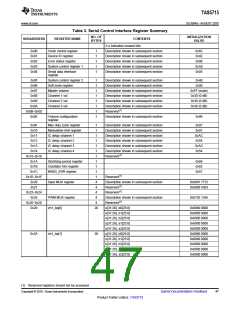
Table 3. Serial Control Interface Register Summary
NO. OF
BYTES
INITIALIZATION
VALUE
SUBADDRESS
REGISTER NAME
CONTENTS
A u indicates unused bits.
0x00
0x01
0x02
0x03
0x04
Clock control register
Device ID register
1
1
1
1
1
Description shown in subsequent section
Description shown in subsequent section
Description shown in subsequent section
Description shown in subsequent section
Description shown in subsequent section
0x6C
0x42
0x00
0xA0
0x05
Error status register
System control register 1
Serial data interface
register
0x05
0x06
System control register 2
Soft mute register
Master volume
1
1
1
1
1
1
1
1
Description shown in subsequent section
Description shown in subsequent section
Description shown in subsequent section
Description shown in subsequent section
Description shown in subsequent section
Description shown in subsequent section
Reserved(1)
0x40
0x00
0x07
0xFF (mute)
0x30 (0 dB)
0x30 (0 dB)
0x30 (0 dB)
0x08
Channel 1 vol
0x09
Channel 2 vol
0x0A
Channel 3 vol
0x0B–0x0D
0x0E
Volume configuration
register
Description shown in subsequent section
0x90
0x0F
0x10
Max duty cycle register
Modulation limit register
IC delay channel 1
IC delay channel 2
IC delay channel 3
IC delay channel 4
1
1
1
1
1
1
1
1
1
1
1
4
4
4
4
4
20
Description shown in subsequent section
Description shown in subsequent section
Description shown in subsequent section
Description shown in subsequent section
Description shown in subsequent section
Description shown in subsequent section
Reserved(1)
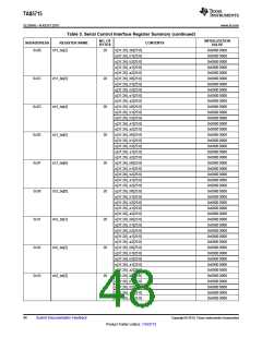
0x97
0x01
0xAC
0x54
0xAC
0x54
0x11
0x12
0x13
0x14
0x15–0x19
0x1A
Start/stop period register
Oscillator trim register
BKND_ERR register
0x68
0x82
0x57
0x1B
0x1C
0x1D–0x1F
0x20
Reserved(1)
Input MUX register
Description shown in subsequent section
Reserved(1)
Reserved(1)
0x0001 7772
0x0000 4303
0x21
0x22–0x24
0x25
PWM MUX register
ch1_bq[0]
Description shown in subsequent section
Reserved(1)
0x0102 1345
0x26–0x28
0x29
u[31:26], b0[25:0]
u[31:26], b1[25:0]
u[31:26], b2[25:0]
u[31:26], a1[25:0]
u[31:26], a2[25:0]
u[31:26], b0[25:0]
u[31:26], b1[25:0]
u[31:26], b2[25:0]
u[31:26], a1[25:0]
u[31:26], a2[25:0]
0x0080 0000
0x0000 0000
0x0000 0000
0x0000 0000
0x0000 0000
0x0080 0000
0x0000 0000
0x0000 0000
0x0000 0000
0x0000 0000
0x2A
ch1_bq[1]
20
(1) Reserved registers should not be accessed.
Copyright © 2010, Texas Instruments Incorporated
Submit Documentation Feedback
47
Product Folder Link(s): TAS5715

 TI [ TEXAS INSTRUMENTS ]