TAS5727
SLOS670 –NOVEMBER 2010
www.ti.com
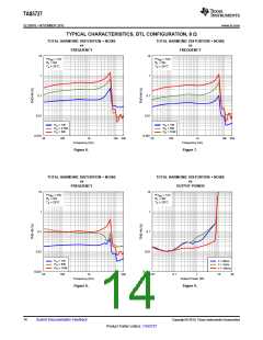
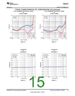
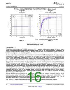
TYPICAL CHARACTERISTICS, BTL CONFIGURATION, 8 Ω (continued)
CROSSTALK
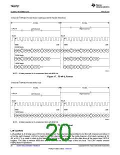
EFFICIENCY
vs
vs
FREQUENCY
TOTAL OUTPUT POWER
0
100
90
80
70
60
50
40
30
20
10
0
VO = 1W
PVDD = 24V
RL = 8Ω
TA = 25°C
Right to Left
Left to Right
−10
−20
−30
−40
−50
−60
−70
−80
−90
−100
PVDD = 12V
PVDD = 18V
PVDD = 24V
RL = 8Ω
TA = 25°C
20
100
1k
10k 20k
0
5
10
15
20
25
30
35
40
Frequency (Hz)
Total Output Power (W)
NOTE: Dashed lines represent thermally limited region.
Figure 14.
Figure 15.
DETAILED DESCRIPTION
POWER SUPPLY
To facilitate system design, the TAS5727 needs only a 3.3-V supply in addition to the (typical) 18-V power-stage
supply. An internal voltage regulator provides suitable voltage levels for the gate drive circuitry. Additionally, all
circuitry requiring a floating voltage supply, e.g., the high-side gate drive, is accommodated by built-in bootstrap
circuitry requiring only a few external capacitors.
In order to provide good electrical and acoustical characteristics, the PWM signal path for the output stage is
designed as identical, independent half-bridges. For this reason, each half-bridge has separate bootstrap pins
(BST_x), and power-stage supply pins (PVDD_x). The gate-drive voltage (GVDD_OUT) is derived from the
PVDD voltage. Special attention should be paid to placing all decoupling capacitors as close to their associated
pins as possible. Inductance between the power-supply pins and decoupling capacitors must be avoided.
For a properly functioning bootstrap circuit, a small ceramic capacitor must be connected from each bootstrap pin
(BST_x) to the power-stage output pin (OUT_x). When the power-stage output is low, the bootstrap capacitor is
charged through an internal diode connected between the gate-drive regulator output pin (GVDD_OUT) and the
bootstrap pin. When the power-stage output is high, the bootstrap capacitor potential is shifted above the output
potential and thus provides a suitable voltage supply for the high-side gate driver. In an application with PWM
switching frequencies in the range from 288 kHz to 384 kHz, it is recommended to use 33-nF, X7R ceramic
capacitors, size 0603 or 0805, for the bootstrap supply. These 33-nF capacitors ensure sufficient energy storage,
even during minimal PWM duty cycles, to keep the high-side power-stage FET (LDMOS) fully turned on during
the remaining part of the PWM cycle.
Special attention should be paid to the power-stage power supply; this includes component selection, PCB
placement, and routing. As indicated, each half-bridge has independent power-stage supply pins (PVDD_x). For
optimal electrical performance, EMI compliance, and system reliability, it is important that each PVDD_x pin is
decoupled with a 100-nF, X7R ceramic capacitor placed as close as possible to each supply pin.
The TAS5727 is fully protected against erroneous power-stage turnon due to parasitic gate charging.
16
Submit Documentation Feedback
Copyright © 2010, Texas Instruments Incorporated
Product Folder Link(s): TAS5727

 TI [ TEXAS INSTRUMENTS ]