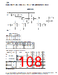
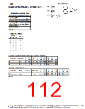
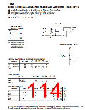
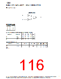
Logic Diagram
1G98
3
1
In0
In1
CONFIGURABLE MULTIPLE-FUNCTION GATE
4
Y
FUNCTION SELECTION TABLE
6
2-to-1 data selector with inverted output
2-input NAND gate
In2
2-input NOR gate with one inverted input
2-input AND gate with one inverted input
2-input NAND gate with one inverted input
2-input OR gate with one inverted input
2-input NOR gate
Noninverted buffer
Inverter
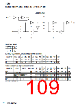
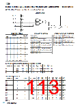
FUNCTION TABLE
INPUTS
OUTPUT
Y
In2 In1 In0
L
L
L
L
L
H
L
H
H
L
L
H
H
L
L
H
L
L
H
H
H
H
H
L
L
H
L
H
H
H
L
H
ELECTRICAL CHARACTERISTICS AND RECOMMENDED OPERATING CONDITIONS
LVC
5V
LVC
3.3V
LVC
2.5V
LVC
1.8V
AUP
3.3V
AUP
2.5V
AUP
1.8V
AUP
1.1V
PARAMETER
MAX or MIN
UNIT
ICC
IOH
IOL
MAX
MAX
MAX
0.01
-32
32
0.01
-24
24
0.01
-8
8
0.01 0.0009 0.0009 0.0009 0.0009
mA
mA
mA
-4
4
-4
4
-3.1
3.1
-1.9
1.9
-1.1
1.1
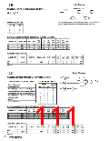
SWITCHING CHARACTERISTICS
LVC
5V
LVC
3.3V
LVC
2.5V
LVC
1.8V
AUP AUP
AUP
1.8V
AUP
1.1V
PARAMETER
INPUT
Any In
OUTPUT
MAX or MIN
MAX
3.3V
2.5V
6
6
7.3
7.3
10.2
10.2
19
19
tPLH
tPHL
5.1
5.1
6.3
6.3
8.3
8.3
14.4
14.4
Y
UNIT:ns
107
PRODUCTION DATA information is current as of publication date. Products conform to specifications per the terms of Texas Instruments standard warranty.
Production processing does not necessarily include testing of all parameters. See www.ti.com/sc/logic for the most current data sheets.

 TI [ TEXAS INSTRUMENTS ]