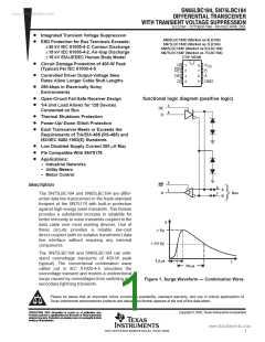
ꢀꢁ ꢂꢃ ꢄ ꢅꢆꢇ ꢈ ꢉ ꢊ ꢀꢁ ꢋꢃ ꢄꢅ ꢆꢇ ꢈꢉ
ꢌꢍ ꢎꢎ ꢏꢐ ꢏꢁꢑ ꢍꢒ ꢄ ꢑ ꢐꢒꢁ ꢀꢆ ꢏ ꢍꢓ ꢏ ꢐ
ꢔ ꢍꢑ ꢕ ꢑ ꢐꢒꢁꢀ ꢍꢏꢁ ꢑ ꢓꢖ ꢄꢑꢒꢗ ꢏ ꢀꢘ ꢙꢙꢐ ꢏꢀ ꢀ ꢍꢖ ꢁ
ꢚ
www.DataSheet4U.com
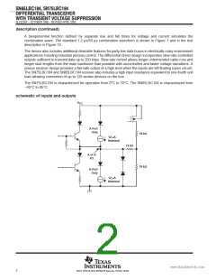
SLLS236F − OCTOBER 1996 − REVISED APRIL 2005
DRIVER SECTION
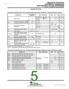
electrical characteristics over recommended operating conditions (unless otherwise noted)
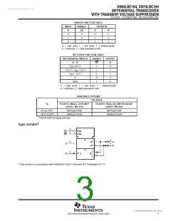
ALTERNATE
SYMBOLS
†
PARAMETER
TEST CONDITIONS
MIN
MAX
25
UNIT
mA
TYP
DE = RE = 5 V, No Load
12
I
Supply current
NA
DE = 0 V,
No Load
RE = 5 V,
CC
175
300
50
µA
I
I
High-level input current (D, DE, RE)
Low-level input current (D, DE, RE)
NA
NA
V = 2.4 V
I
µA
µA
IH
V = 0.4 V
I
−50
IL
V
V
V
= −7 V
−250 −120
O
O
O
Short-circuit output current
(see Note 5)
I
NA
= V
CC
250
250
mA
OS
OZ
= 12 V
I
High-impedance output current
Output voltage
NA
See Receiver I
mA
V
I
V
V
V
V
, V
oa ob
0
V
CC
I
O
= 0
O
Peak-to-peak change in common-
mode output voltage during state
transitions
See Figures 5 and 6
0.8
V
NA
OC(PP)
OC
Common-mode output voltage
|V
os
|
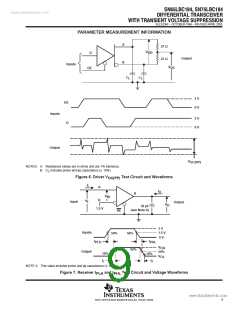
See Figure 4
See Figure 5
1
3
0.1
6
V
V
Magnitude of change, common-
mode steady-state output voltage
|∆V
OC(SS)
|
|V − V |
os os
I
O
= 0
1.5
1.5
V
V
Magnitude of differential output
voltage |V − V |
|V
|
V
o
OD
R
= 54 Ω,
See Figure 4
A
B
L
L
Change in differential voltage mag-
nitude between logic states
∆|V
|
||V | − |V ||
R
= 54 Ω
0.1
V
OD
t
t
†
All typical values are measured with T = 25°C and V
CC
= 5 V.
A
NOTE 5: This parameter is measured with only one output being driven at a time.
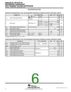
switching characteristics over recommended operating conditions (unless otherwise noted)
PARAMETER
TEST CONDITIONS
MIN
TYP
MAX
1.3
1.3
1.3
1.3
150
1.2
1.2
3.5
3.5
2
UNIT
µs
µs
µs
µs
ns
t
t
t
t
t
t
t
t
t
t
t
Differential output delay time, low-to-high-level output
Differential-output delay time, high-to-low-level output
Propagation delay time, low-to-high-level output
Propagation delay time, high-to-low-level output
d(DH)
d(DL)
PLH
PHL
sk(p)
r
0.5
0.5
75
R
= 54 Ω,
C = 50 pF,
L
L
See Figure 5
Pulse skew (|t |)
− t
d(DH) d(DL)
Rise time, single ended
Fall time, single ended
0.25
0.25
µs
µs
µs
µs
µs
µs
f
Output enable time to high level
Output enable time to low level
Output disable time from high level
Output disable time from low level
R
R
R
R
= 110 Ω,
= 110 Ω,
= 110 Ω,
= 110 Ω,
See Figure 2
See Figure 3
See Figure 2
See Figure 3
PZH
PZL
PHZ
PLZ
L
L
L
L
2
5
POST OFFICE BOX 655303 • DALLAS, TEXAS 75265

 TI [ TEXAS INSTRUMENTS ]