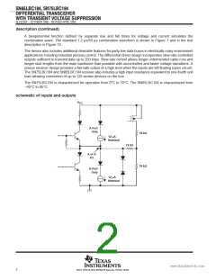
ꢀ ꢁꢂ ꢃꢄ ꢅ ꢆ ꢇꢈ ꢉꢊ ꢀꢁꢋ ꢃ ꢄ ꢅꢆꢇ ꢈ ꢉ
ꢚ
ꢌ ꢍ ꢎ ꢏꢐ ꢏꢁ ꢑ ꢍ ꢒꢄ ꢑꢐ ꢒꢁ ꢀꢆ ꢏꢍ ꢓ ꢏ ꢐ
www.DꢎataSheet4U.com
ꢔꢍ ꢑ ꢕ ꢑ ꢐ ꢒꢁ ꢀꢍ ꢏꢁ ꢑ ꢓ ꢖꢄꢑꢒꢗ ꢏ ꢀ ꢘꢙ ꢙꢐ ꢏꢀ ꢀꢍ ꢖ ꢁ
SLLS236F − OCTOBER 1996 − REVISED APRIL 2005
description (continued)
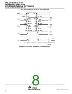
A biexponential function defined by separate rise and fall times for voltage and current simulates the
combination wave. The standard 1.2 µs/50 µs combination waveform is shown in Figure 1 and in the test
description in Figure 15.
The device also includes additional desirable features for party-line data buses in electrically noisy environment
applications including industrial process control. The differential-driver design incorporates slew-rate-controlled
outputs sufficient to transmit data up to 250 kbps. Slew-rate control allows longer unterminated cable runs and
longer stub lengths from the main backbone than possible with uncontrolled and faster voltage transitions. A
unique receiver design provides a fail-safe output of a high level when the inputs are left floating (open circuit).
The SN75LBC184 and SN65LBC184 receiver also includes a high input resistance equivalent to one-fourth unit
load allowing connection of up to 128 similar devices on the bus.
The SN75LBC184 is characterized for operation from 0°C to 70°C. The SN65LBC184 is characterized from
−40°C to 85°C.
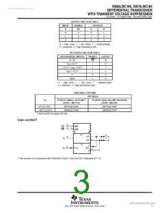
schematic of inputs and outputs
V
CC
A Port
Only
16 kΩ
12 µA
Nominal
72 kΩ
A or B
I/O
16 kΩ
B Port
Only
12 µA
Nominal
2
POST OFFICE BOX 655303 • DALLAS, TEXAS 75265

 TI [ TEXAS INSTRUMENTS ]