RM46L450
RM46L850
SPNS184 –SEPTEMBER 2012
www.ti.com
5.4 Multi-Buffered 12bit Analog-to-Digital Converter
The multibuffered A-to-D converter (MibADC) has a separate power bus for its analog circuitry that
enhances the A-to-D performance by preventing digital switching noise on the logic circuitry which could
be present on VSS and VCC from coupling into the A-to-D analog stage. All A-to-D specifications are given
with respect to ADREFLO unless otherwise noted.
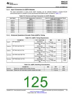
Table 5-15. MibADC Overview
Description
Resolution
Value
12 bits
Assured
Monotonic
Output conversion code
00h to 3FFh [00 for VAI ≤ ADREFLO; 3FFh for VAI ≥ ADREFHI]
5.4.1 Features
•
•
•
•
•
•
•
•
•
•
•
•
•
•
12-bit resolution
ADREFHI and ADREFLO pins (high and low reference voltages)
Total Sample/Hold/Convert time: 600ns Minimum at 30MHz ADCLK
One memory region per conversion group is available (event, group 1, group 2)
Allocation of channels to conversion groups is completely programmable
Supports flexible channel conversion order
Memory regions are serviced either by interrupt or by DMA
Programmable interrupt threshold counter is available for each group
Programmable magnitude threshold interrupt for each group for any one channel
Option to read either 8-bit, 10-bit or 12-bit values from memory regions
Single or continuous conversion modes
Embedded self-test
Embedded calibration logic
Enhanced power-down mode
–
Optional feature to automatically power down ADC core when no conversion is in progress
•
External event pin (ADxEVT) programmable as general-purpose I/O
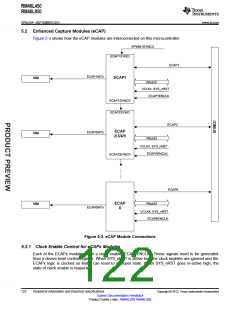
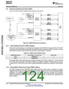
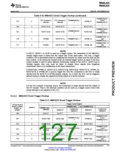
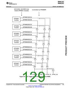
5.4.2 Event Trigger Options
The ADC module supports 3 conversion groups: Event Group, Group1 and Group2. Each of these 3
groups can be configured to be hardware event-triggered. In that case, the application can select from
among 8 event sources to be the trigger for a group's conversions.
5.4.2.1 MIBADC1 Event Trigger Hookup
Table 5-16. MIBADC1 Event Trigger Hookup
Trigger Event Signal
Group Source
Select, G1SRC,
G2SRC or
EVSRC
PINMMR30[0] = 0 and PINMMR30[1] = 1
Event #
PINMMR30[0] = 1
(default)
Control for
Option B
Option A
Control for
Option B
Option A
000
001
010
1
2
3
AD1EVT
N2HET1[8]
N2HET1[10]
AD1EVT
—
PINMMR30[8] = 1
—
AD1EVT
—
PINMMR30[8] = 0
and
PINMMR30[9] = 1
N2HET2[5]
ePWM_B
N2HET1[27]
N2HET1[27]
—
126
Peripheral Information and Electrical Specifications
Copyright © 2012, Texas Instruments Incorporated
Submit Documentation Feedback
Product Folder Links: RM46L450 RM46L850

 TI [ TEXAS INSTRUMENTS ]