Application Notes
PT6920/PT6930 Series
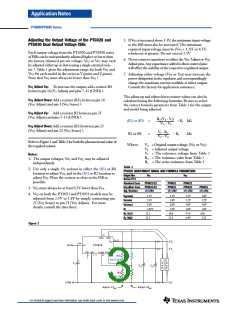
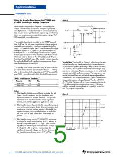
Figure 1
Using the Standby Function on the PT6920 and
PT6930 Dual Output Voltage Converters
22
V2(sns)
1
Both output voltages of the 23-pin PT6920/6930 dual
output converter may be disabled using the regulator’s
standby function. This function may be used in applications
that require power-up/shutdown sequencing, or wherever
there is a requirement to control the output voltage On/
Off status with external circuitry.
V1(sns)
18
12
-
-
21
15
V2out
V2out
V1out
4,5,6
Vin
Vin
PT6921
V1out
GND
7
Vo2(adj) V01(adj)
23 16
STBY
3
- 11
+
C1
+
+
C2
C3
The standby function is provided by the STBY* control
(pin 3). If pin 3 is left open-circuit the regulator operates
normally, and provides a regulated output at both Vo1
(pins 12–15) and Vo2 (pins 18–21) whenever a valid supply
voltage is applied to Vin (pins 4, 5, & 6) with respect to
COM
COM
Q1
BSS138
Inhibit
+5V V in
2
GND (pins 7–11). If a low voltage is then applied to pin 3,
both regulator outputs will be simultaneously disabled and
the input current drawn by the ISR will typcially drop to
less than 30mA (50mA max). The standby control may also
be used to hold-off both regulator outputs during the pe-
riod that input power is applied.
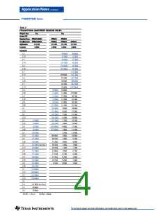
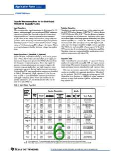
Turn-On Time: Turning Q1 in Figure 1 off removes the low-
voltage signal at pin 3 and enables both outputs from the
PT6920/6930 regulator. Following a delay of about 10–20ms,
Vo1 and Vo2 rise together until the lower voltage, Vo2,
reaches its set output. Vo1 then continues to rise until both
outputs reach full regulation voltage. The total power-up
time is less than 25ms, and is relatively independant of load,
temperature, and output capacitance. Figure 2 shows wave-
forms of the output voltages Vo1 and Vo2, for a PT6931
(3.3V/2.5V). The turn-off of Q1 corresponds to the rise in
Vstby. The waveforms were measured with a 5Vdc input
voltage, and with resistive loads of 5A and 2A at the Vo1
and Vo2 outputs respectively.
The standby pin is ideally controlled using an open-collector
(or open-drain) discrete transistor (See Figure 1). It may
3
also be driven directly from a dedicated TTL compatible
gate. Table 1 provides details of the threshold requirements.
2,3
Table 1 Inhibit Control Thresholds
Parameter
Min
Max
Enable (V )
IH
1.8V
Vin
Disable (V )
IL
–0.1V
0.8V
Notes:
1. The Standby/Inhibit control logic is similar for all
Power Trends’ modules, but the flexibility and
threshold tolerances will be different. For specific
information on this function for other regulator
models, consult the applicable application note.
Figure 2
Vo1 (3.3V)
Vo2 (2.5V)
2. The Standby control pin is ideally controlled using an
open-collector (or open-drain) discrete transistor and
requires no external pull-up resistor. To disable the
regulator output, the control pin must be pulled to
less than 0.8Vdc with a low-level 0.5mA sink to
ground.
3. The Standby input on the PT6920/6930 series may
be driven by a differential output device, making it
directly compatible with TTL logic. The control
input has an internal pull-up to the input voltage Vin.
A voltage of 1.8V or greater ensures that the
Vstby
Ch1 1V/Div
Timebase: 5ms/Div
Ch2 1V/Div
Ch3 5V/Div
regulator is enabled. Do not use devices that can drive
the Standby control input above 5.5V or Vin.
For technical support and more information, see inside back cover or visit www.ti.com

 TI [ TEXAS INSTRUMENTS ]