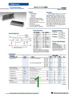
PT6930 Series
8-A5V-Input Dual-Output
Integrated Switching Regulator
SLTS062B
(Revised 7/20/2001)
Features
• Dual Outputs:
Description
The PT6930 Excalibur™ series of 8-A
dual-output ISRs are designed to power
DSP ICs. Both output voltages are inde-
pendently adjustable with external resistors.
The second output may also be set to an
alternate lower bus voltage with a simple
pin strap. Internal power sequencing of
both outputs, during both power-up and
power-down, meets the requirements of
most DSP chipsets.
+3.3V/2.5V
+3.3V/1.5V
+3.3V/1.8V
• Adjustable Output Voltages
• Remote Sense (both outputs)
• Standby Function
• Over-Temperature Protection
• Soft-Start
• Internal Sequencing
• 23-pin Excalibur™ Package
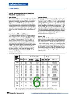
Pin-Out Information
Pin Function
Ordering Information
PT 6931o = +3.3 Volts
Pin Function
+2.5/1.8 Volts
PT 6932o = +3.3 Volts
+1.5/1.2 Volts
PT 6933o = +3.3 Volts
+1.8/1.2 Volts
Standard Application
1
2
Vo1 Sense
No Connect
STBY
VIN
13
14
15
16
17
18
19
20
21
22
23
Vo1
Vo2 Sense
Vo1 Sense
Vo1
3
Vo1
STBY
4
Vo1 Adjust
No Connect
Vo2
3
22
1
Vo2
Vo1
18-21
12-15
5
VIN
VIN
4,5,6
PT6930
6
VIN
7
GND
GND
GND
GND
GND
Vo1
Vo2
+
PT Series Suffix
(PT1234X)
7-11
16
23
C3
+
C1
8
Vo2
Case/Pin
Configuration
C2
9
Vo2
GND
GND
Vertical Through-Hole
Horizontal Through-Hole
Horizontal Surface Mount
N
A
C
10
11
12
Vo2 Sense
Vo2 Adjust*
C1/C2 =Req’d 330µF electrolytic (See table footnotes)
C3 =Optional 100µF electrolytic
(For dimensions and PC board layout, see
Package Styles 1320 and 1330).
* Note:Vo1 & Vo2 Adjust can be pin-strapped to an
alternative lower bus voltage. Consult the voltage
adjustment application note for more information.
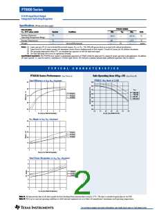
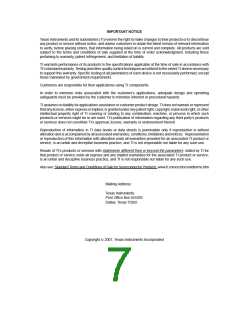
Specifications
PT6930 SERIES
Characteristics
(Ta= 25°C unless noted)
Symbols
Conditions
Min
Typ
Max
Units
(1)
(2)
Output Current
Io1, Io2
Ta = +60°C, 200 LFM, pkg N
Ta = +25°C, natural convection
0.1A ≤ Io ≤ Ityp
Vo1 =3.3V
Vo2 =2.5V
Vo2 =1.8V
Vo2 =1.5V
Vo1 =1.2V
0.1
—
5.5
(2)
(2)
(2)
(2)
0
0
0
0
—
—
—
—
2.2
1.75
1.45
1.2
A
(1)
(2)
(2)
(2)
(2)
(2)
Vo1 =3.3V
Vo2 =2.5V
Vo2 =1.8V
Vo2 =1.5V
Vo1 =1.2V
0.1
0
—
—
—
—
—
6.0
A
A
2.2
0
1.75
1.45
1.2
0
0
Input Voltage Range
Vin
4.5
—
5.5
V
V
Output Voltage Tolerance
∆Vo
Vin = +5V, Io =Ityp, both outputs
Vo-0.1
—
Vo+0.1
0°C ≤ Ta ≤ +65°C
Line Regulation
Load Regulation
Vo Ripple/Noise
Regline
Regload
Vn
4.5V ≤ Vin ≤ 5.5V, Io =Ityp
Vin = +5V, 0.1 ≤ Io ≤ Ityp
Vin = +5V, Io =Ityp
Vo1
Vo2
—
—
7
7
17
13
V
Vo1
Vo2
—
—
17
33
10
mV
4
Vo1
Vo2
—
—
50
25
—
—
mV
Transient Response
with C2 = 330µF
ttr
Io step between 0.5xItyp and Ityp
Vo over/undershoot
—
—
—
25
60
60
—
—
—
µSec
mV
Vos
Vo1
Vo2
Efficiency
η
Vin = +5V, Io =4A total
—
75
—
%
Switching Frequency
ƒo
4.5V ≤ Vin ≤5.5V
0.1A ≤ Io ≤ Ityp
600
725
475
kHz
(Continued)
For technical support and more information, see inside back cover or visit www.ti.com

 TI [ TEXAS INSTRUMENTS ]