Application Notes
PT6880 Series
Using the On/Off Standby Function on the
PT6880 Excalibur™ Series of ISRs
The PT6880 series of integrated switching regulators
(ISRs) incorporate an on/off standby function, which
may be used to disable the regulator output. This func-
tion is provided by the STBY* control (pin 4). If pin 4 is left
open-circuit the regulator operates normally, providing a
regulated output whenever a valid supply voltage is applied
to Vin (pins 8–10) with respect to GND (pins 6, 7, & 11–
14). If the STBY* control is driven low to ground 1, the
regulator output is disabled and the input current drawn
by the ISR drops to its idle value 2.
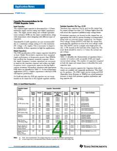
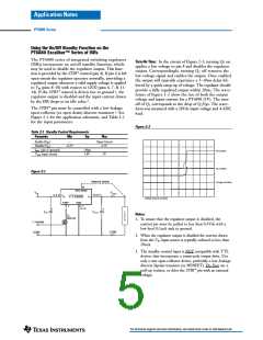
Turn-On Time: In the circuit of Figure 2-1, turning Q1 on
applies a low voltage to pin 4 and disables the regulator
output. Correspondingly, turning Q1 off removes the
low-voltage signal and enables the output. Once enabled
the output will typically experience a 5–10ms delay fol-
lowed by a quick ramp-up of voltage. The regulator should
provide a fully regulated output within 20ms. The wave-
forms of Figure 1-2 show the rise of both the output
voltage and input current for a PT6883 (5V). The turn
off of Q1 corresponds to the drop of Q1Vgs. The wave-
form was measured with a 24Vdc input voltage and 4-ADC
load.
The STBY* pin must be controlled with a low-leakage
open-collector (or open-drain) discrete transistor 3. See
Figure 2-1 for the application schematic, and Table 2-1
for the input parameters.
Figure 2-2
Table 2-1 Standby Control Requirements
Parameter
Min
Typ
Max
Enable (VIH
Disable (VIL
)
)
—
–0.2V
Open Circuit
0.3V
Istby (pin 4 =ground)
Vstby (open circuit)
–50µA
1.4V
Vo (2V/Div)
2V
Iin (1A/Div)
Figure 2-1
REMOTE SENSE
Q1Vgs (10V/Div)
18
Rem Sense
VIN
VOUT
15,16,17
8, 9,10
VIN
VO
PT6880
HORIZ SCALE: 5ms/Div
STBY*
4
GND
6, 7,
11–14
+
+
L
O
A
D
CIN
C O U T
Notes:
Q1
BSS138
1. To ensure that the regulator output is disabled, the
control pin must be pulled to less than 0.3Vdc with a
low-level 0.1mA sink to ground.
1 =Inhibit
COM
COM
2. When the regulator output is disabled the current drawn
from the Vin input source is typically reduced to less than
20mA.
3. The standby control input is NOT compatible with TTL
devices that incorporate a totem-pole output drive. Use
only a true open-collector device, preferably a low-leakage
discrete bipolar transistor (or MOSFET). Do Not use a
pull-up resistor, or drive the STBY* pin with an external
voltage.
For technical support and more information, see inside back cover or visit www.ti.com

 TI [ TEXAS INSTRUMENTS ]