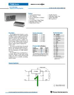
PT6880 Series
5-A, 15-36-V Input
Integrated Switching Regulator
SLTS103B -JULY 2000 - REVISED JANUARY 2003
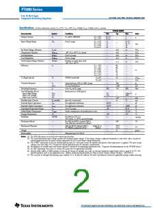
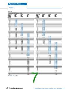
Specifications (Unless otherwise stated, Ta =25°C, Vin =28V, Cin =560µF, Cout =330µF, and Io =Iomax)
PT6880 SERIES
Characteristic
Symbol
Conditions
Min
Typ
Max
Units
(1)
(1)
Output Current
Io
Ta =60°C, 200LFM
Vo ≤ 12V
0.1
0.1
—
—
5
4
A
Vo > 12V
(2)
(2)
Input Voltage Range
Vin
Over Io range
Vo =2.5V
Vo =3.3V
Vo =5.0V
Vo ≥6.5V
15
15
15
18
—
—
—
—
25
33
36
36
Vdc
Set Point Voltage Tolerance
Temperature Variation
Line Regulation
Load Regulation
Total Output Voltage Variation
Vo tol
—
—
—
—
0.5
0.5
0.5
0.5
1
—
1
%Vo
%Vo
%Vo
%Vo
Regtemp
Regline
Regload
∆Votot
–40° ≤Ta ≤ +85°C, Io =Iomin
Over Vin range
Over Io range
Includes set-point, line, load,
–40° ≤Ta ≤ +85°C
1
—
1.5
2
%Vo
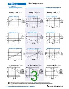
Efficiency
η
Vo = 15V
Vo = 12V
Vo =9.0V
Vo =5.0V
Vo =3.3V
Vo =2.5V
—
—
—
—
—
—
90
88
87
82
73
78
—
—
—
—
—
—
%
Vo Ripple (pk-pk)
Transient Response
Switching Frequency
Vr
20MHz bandwidth
Vo≤5V
Vo>5V
—
—
—
—
500
50
1
100
100
550
—
—
—
—
600
mVpp
%Vo
µs
mV
kHz
ttr
∆Vtr
ƒs
5A/µs load step, 50% to 100% Iomax
Vo over/undershoot
Over Vin and Io range
On/Off Standby (Pin 4)
Input High Voltage
Input Low Voltage
Input Low Current
Referenced to GND (pin 6)
(3)
VIH
VIL
IIL
2.0
—
—
–0.5
16
—
—
—
—
—
Open
+0.4
–
35
—
V
–0.1
—
mA
mA
µF
Standby Input Current
External Input Capacitance
External Output Capacitance
Operating Temperature Range
Solder Reflow Temperature
Storage Temperature
Iin standby
Cin
Cout
pins 4 & 6 connected
See application schematic
See application schematic
Over Vin range
Surface temperature of module pins or case
—
—
(4)
(4)
560
330
–40
—
1,000
µF
(5)
T
85
°C
°C
°C
a
(6)
Treflow
T
s
215
125
–40
Reliability
MTBF
Per Bellcore TR-332
6
7.7
—
—
—
—
10 Hrs
50% stress, Ta =40°C, ground benign
Mechanical Shock
—
Per Mil-Std-883D, method 2002.3,
1ms, half-sine, mounted to a fixture
500
G’s
(7)
(7)
Mechanical Vibration
—
Mil-Std-883D, Method 2007.2,
20-2000Hz, soldered in PCB
Suffix N, A
Suffix C
—
—
20
—
—
G’s
15
Weight
Flammability
—
—
—
23
—
grams
Materials meet UL 94V-0
Notes: (1) The ISR will operate at no load with reduced specifications.
(2) The stated maximum input voltage assumes the nominal output voltage. If the output voltage is adjusted (trimmed) to some other value, consult the
related application note on output voltage adjustment for the revised input voltage limitations.
(3) The STBY* control (pin 4) has an internal pull-up and if it is left open circuit the module will operate when input power is applied. The open-circuit
voltage is low (less than 5V). Consult the related application note for interface considerations.
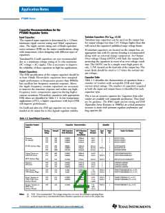
(4) For guidance on suitable input and output capacitors consult the accompanying application note, “Capacitor Recommendations for the PT6880 Series.”
(5) See Safe Operating Area curves or contact the factory for the appropriate derating.
(6) During solder reflow of SMD package version do not elevate the module case, pins, or internal component temperatures above a peak of 215°C. For
further guidance refer to the application note, “Reflow Soldering Requirements for Plug-in Power Surface Mount Products,” (SLTA051).
(7) The case pins on through-hole package types (suffixes N & A) must be soldered. For more information consult the applicable package outline drawing.
For technical support and more information, see inside back cover or visit www.ti.com

 TI [ TEXAS INSTRUMENTS ]