PCM9211
SBAS495 –JUNE 2010
MPIO Description
Overview
www.ti.com
The PCM9211 offers significant flexibility through its MPIO pins. Depending on the system partitioning of the
specific end product, the pins can be reconfigured to offer various I/Os that complement the design.
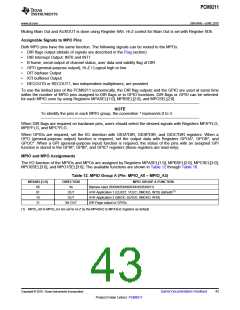
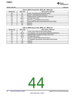
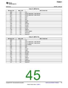
There are 14 flexible pins: 12 are Input/Output pins, and two pins that are output only.
The 12 multi-purpose I/O (MPIO) pins are grouped into three banks, each with four pins: MPIO_A, MPIO_B, and
MPIO_C.
The two multi-purpose outputs (MPO) pins are assigned as MPO0 and MPO1.
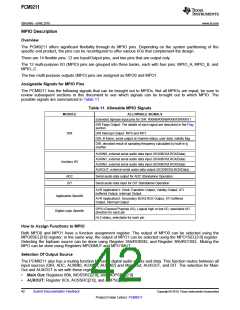
Assignable Signals for MPIO Pins
The PCM9211 has the following signals that can be brought out to MPIOs. Not all MPIOs are equal; be sure to
review subsequent sections in this document to see which signals can be brought out to which MPIO. The
possible signals are summarized in Table 11.
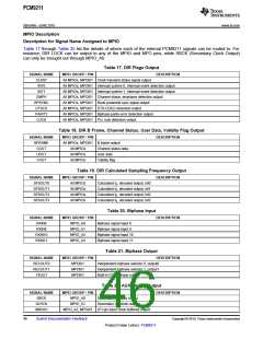
Table 11. Allowable MPIO Signals
MODULE
ALLOWABLE SIGNALS
Extended biphase input pins for DIR: RXIN8/RXIN9/RXIN10/RXIN11
DIR Flags Output: The details of each signal are described in the Flag
section.
DIR
DIR Interrupt Output: INT0 and INT1
DIR, B frame, serial output of channel status, user data, validity flag
DIR, decoded result of sampling frequency calculated by built-in fS
counter
AUXIN0, external serial audio data input (SCK/BCK/LRCK/Data)
AUXIN1, external serial audio data input (SCK/BCK/LRCK/Data)
AUXIN2, external serial audio data input (SCK/BCK/LRCK/Data)
AUXOUT, external serial audio data output (SCK/BCK/LRCK/Data)
Auxiliary I/O
ADC
DIT
Serial audio data output for ADC Standalone Operation
Serial audio data input for DIT Standalone Operation
AVR Application1: Clock Transition Output, Validity Output, XTI
buffered Output, Interrupt Output
Application-Specific
Digital Logic Specific
AVR Application2: Secondary BCK/LRCK Output, XTI buffered
Output, Interrupt Output
GPIO (General Purpose I/O), Logical high or low I/O, selectable I/O
direction for each pin
Hi-Z status, selectable for each pin
How to Assign Functions to MPIO
Both MPO0 and MPO1 have a function assignment register. The output of MPO0 can be selected using the
MPO0SEL[3:0] register; in the same way, the output of MPO1 can be selected using the MPO1SEL[3:0] register.
Selecting the biphase source can be done using Register 35h/RO0SEL and Register 36h/RO1SEL. Muting the
MPO can be done using Registers MPO0MUT and MPO1MUT.
Selection Of Output Source
The PCM9211 also has a routing function for serial digital audio clocks and data. This function routes between all
input sources (DIR, ADC, AUXIN0, AUXIN1, AUXIN2) and Main Out, AUXOUT, and DIT. The selection for Main
Out and AUXOUT is set with these registers:
•
•
Main Out: Registers 6Bh, MOSSRC[2:0], and MOPSRC[2:0]
AUXOUT: Register 6Ch, AOSSRC[2:0], and AOPSC[2:0]
42
Submit Documentation Feedback
Copyright © 2010, Texas Instruments Incorporated
Product Folder Link(s): PCM9211

 TI [ TEXAS INSTRUMENTS ]