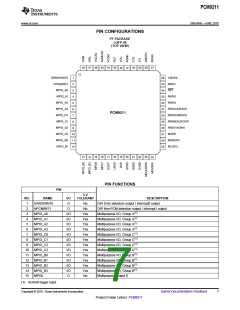
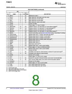
PCM9211
www.ti.com
SBAS495 –JUNE 2010
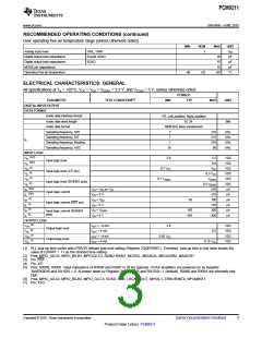
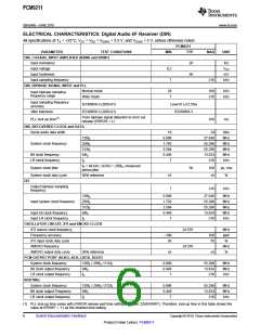
RECOMMENDED OPERATING CONDITIONS (continued)
Over operating free-air temperature range (unless otherwise noted).
MIN
NOM
MAX
UNIT
VPP
pF
Analog input level
VINL, VINR
Except SCKO
SCKO
3
Digital output load capacitance
Digital output load capacitance
MODE pin capacitance
20
10
pF
10
pF
Operating free-air temperature
–40
+25
+85
°C
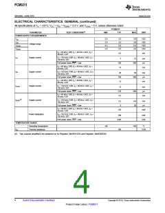
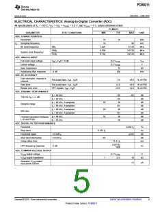
ELECTRICAL CHARACTERISTICS: GENERAL
All specifications at TA = +25°C, VCC = VDD = VDDRX = 3.3 V, and VCCAD = 5 V, unless otherwise noted.
PCM9211
PARAMETER
DIGITAL INPUT/OUTPUT
TEST CONDITIONS(1)
MIN
TYP
MAX
UNIT
DATA FORMAT
I2S, Left-Justified, Right-Justified
Audio data interface format
Audio data word length
Audio data format
16, 24
Bits
MSB first, twos complement
Sampling frequency, DIR
Sampling frequency, DIT
Sampling frequency, Routing
Sampling frequency, ADC
7
7
216
216
216
96
kHz
kHz
kHz
kHz
fS
7
16
INPUT LOGIC
(2)(3)
VIH
2.0
0.7 VCC
5.5
0.8
VDC
VDC
VDC
VDC
VDC
VDC
mA
Input logic level
(2)(3)
VIL
(4)
VIH
VCC
Input logic level (XTI pin)
Input logic level (RXIN0/1 pins)
Input logic current
(4)
VIL
0.3 VCC
VDDRX
(5)
VIH
0.7 VDDRX
(5)
VIL
0.3 VDDRX
±10
(2)(4)
IIH
VIN = VDD or VCC
(2)(4)
IIL
VIN = 0 V
VIN = VDD
VIN = 0 V
VIN = VDDRX
VIN = 0 V
±10
mA
(3)
IIH
65
100
mA
Input logic current (RST pin)
(3)
IIL
±10
mA
(5)
IIH
165
300
mA
Input logic current (RXIN0/1
pins)
(5)
IIL
–165
–300
mA
OUTPUT LOGIC
(6)
VOH
IOUT = –4 mA
IOUT = 4 mA
IOUT = –4 mA
IOUT = 4 mA
2.8
VDC
VDC
VDC
VDC
Output logic level
Output logic level
(6)
VOL
0.5
(7)
VOH
0.85 VCC
(7)
VOL
0.15 VCC
(1) PLL lock-up time varies with ERROR release wait time setting (Register 23h/ERRWT). Therefore, lock-up time in this table shows the
value at ERRWT = 11 as the shortest time setting.
(2) Pins: MPIO_A0-A3, MPIO_B0-B3, MPIOC0-C3, RXIN2-RXIN7, MC/SCL, MDI/SDA, MDO/ADR0, MS/ADR1
(3) Pin: RST
(4) Pin: XTI
(5) Pins: RXIN0, RXIN1. Input impedance of RXIN0 and RXIN1 is 20 kΩ (typical). COAX amplifiers are powered on by Register
34h/RX0DIS and RX1DIS = 0. At power down by Register 34h/RX0DIS and RX1DIS= 1 (default), RXIN0 and RXIN1 are internally tied
high.
(6) Pins: MPIO_A0-A3, MPIO_B0-B3, MPIO_C0-C3, SCKO, BCK, LRCK, DOUT, MPO0-1, ERROR/INT0, NPCM/INT1.
(7) Pin: XTO.
Copyright © 2010, Texas Instruments Incorporated
Submit Documentation Feedback
3
Product Folder Link(s): PCM9211

 TI [ TEXAS INSTRUMENTS ]