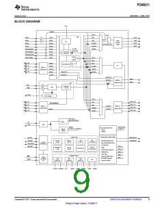
PCM9211
SBAS495 –JUNE 2010
www.ti.com
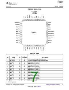
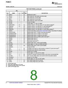
PIN FUNCTIONS (continued)
PIN
5-V
NO.
16
17
18
19
20
21
22
23
24
25
26
27
28
29
30
31
32
33
34
35
36
37
38
39
40
41
42
43
44
45
46
47
48
NAME
I/O
O
O
O
O
O
–
–
I/O
I/O
I
TOLERANT
DESCRIPTION
MPO1
No
No
No
No
No
–
Multipurpose output 1
DOUT
Main output port, serial digital audio data output
Main output port, LR clock output
LRCK
BCK
Main output port, Bit clock output
SCKO
Main output port, System clock output
DGND
Ground, for digital
DVDD
–
Power supply, 3.3 V (typ.), for digital
MDO/ADR0
MDI/SDA
MC/SCL
MS/ADR1
MODE
Yes
Yes
Yes
Yes
No
Yes
Yes
Yes
Yes
Yes
Yes
Yes
Yes
–
Software control I/F, SPI data output / I2C slave address setting0(2)
Software control I/F, SPI data input / I2C data input/output(2)(3)
Software control I/F, SPI clock input / I2C clock input(2)
Software control I/F, SPI chip select / I2C slave address setting1(2)
I
I
Control mode setting, (see the Serial Control Mode section, Control Mode Pin Setting)
Biphase signal, input 7 / AUXIN0, serial audio data input(2)
Biphase signal, input 6 / AUXIN0, LR clock input(2)
Biphase signal, input 5 / AUXIN0, bit clock input(2)
Biphase signal, input 4 / AUXIN0, system clock input(2)
Biphase signal, input 3(2)
RXIN7/ADIN0
I
RXIN6/ALRCKI0
RXIN5/ABCKI0
RXIN4/ASCKI0
RXIN3
I
I
I
I
RXIN2
I
Biphase signal, input 2(2)
Reset Input, active low(2)(4)
RST
I
RXIN1
I
Biphase signal, input 1, built-in coaxial amplifier
Power supply, 3.3 V (typ.), for RXIN0 and RXIN1.
Biphase signal, input 0, built-in coaxial amplifier
Ground, for RXIN
Oscillation circuit input for crystal resonator or external XTI clock source input(5)
Oscillation circuit output for crystal resonator
Ground, for PLL analog
VDDRX
RXIN0
–
I
Yes
-
GNDRX
XTI
-
I
No
No
–
XTO
O
–
–
O
O
–
–
I
AGND
VCC
–
Power supply, 3.3 V (typ.), for PLL analog
FILT
No
No
–
External PLL loop filter connection terminal; must connect recommended filter
ADC common voltage output; must connect external decoupling capacitor
Ground, for ADC analog
VCOM
AGNDAD
VCCAD
VINL
–
Power supply, 5.0 V (typ.), for ADC analog
ADC analog voltage input, left channel
No
No
VINR
I
ADC analog voltage input, right channel
(2) Schmitt trigger input
(3) Open-drain configuration in I2C mode
(4) Onboard pull-down resistor (50 kΩ, typical)
(5) CMOS Schmitt trigger input
8
Submit Documentation Feedback
Copyright © 2010, Texas Instruments Incorporated
Product Folder Link(s): PCM9211

 TI [ TEXAS INSTRUMENTS ]