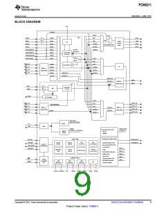
PCM9211
SBAS495 –JUNE 2010
www.ti.com
This integrated circuit can be damaged by ESD. Texas Instruments recommends that all integrated circuits be handled with
appropriate precautions. Failure to observe proper handling and installation procedures can cause damage.
ESD damage can range from subtle performance degradation to complete device failure. Precision integrated circuits may be more
susceptible to damage because very small parametric changes could cause the device not to meet its published specifications.
PACKAGE/ORDERING INFORMATION(1)
OPERATING
PACKAGE
DESIGNATOR
TEMPERATURE
RANGE
PACKAGE
MARKING
ORDERING
NUMBER
TRANSPORT MEDIA,
QUANTITY
PRODUCT
PACKAGE-LEAD
PCM9211PT
Tray, 250
PCM9211
LQFP-48
PT
–40°C to +85°C
PCM9211
PCM9211PTR
Tape and Reel, 1000
(1) For the most current package and ordering information, see the Package Option Addendum at the end of this document, or see the
device product folder on www.ti.com.
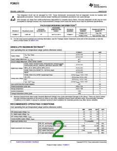
ABSOLUTE MAXIMUM RATINGS(1)
Over operating free-air temperature range (unless otherwise noted).
PCM9211
–0.3 to +4.0
–0.3 to +6.5
±0.1
UNIT
VCC, VDD, VDDRX
VCCAD
V
V
V
V
Supply voltage
Supply voltage differences: VCC, VDD
Ground voltage differences: AGND, DGND, GNDRX
±0.1
RXIN2, RXIN3, RXIN4/ASCKI0, RXIN5/ABCKI0, RXIN6/ALRCKI0,
RXIN7/ADIN0, MC/SCL, MDI/SDA, MDO/ADR, MS/ADR1, RST
–0.3 to +6.5
V
MPIO_A0-A3, MPIO_B0-B3, MPIO_C0-C3
–0.3 to +6.5
–0.3 to +6.5
V
V
Digital input voltage
Analog input voltage
RXIN0, RXIN1 (For S/PDIF TTL / OPTICAL input)
MODE
–0.3 to +4.0
V
RXIN0, RXIN1 (For S/PDIF Coaxial Input Only)
–0.3 to (VDDRX + 0.3) < +4.0
–0.3 to (VDD + 0.3) < +4.0
–0.3 to (VCC + 0.3) < +4.0
–0.3 to (VCCAD + 0.3) < +6.5
±10
V
XTI, XTO
FILT
V
V
VINL, VINR, VCOM
V
Input current (any pins except supplies)
Ambient temperature under bias
Storage temperature
mA
°C
°C
°C
°C
–40 to +125
–55 to +150
Junction temperature
+150
Package temperature (reflow, peak)
+260
(1) Stresses beyond those listed under Absolute Maximum Ratings may cause permanent damage to the device. These are stress ratings
only and functional operation of the device at these or any other conditions beyond those indicated under Recommended Operating
Conditions is not implied. Exposure to absolute-maximum-rated conditions for extended periods may affect device reliability.
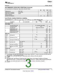
RECOMMENDED OPERATING CONDITIONS
Over operating free-air temperature range (unless otherwise noted).
MIN
2.9
2.9
4.5
2.9
NOM
3.3
MAX
3.6
UNIT
DIR analog supply voltage, VCC
ALL digital supply voltage, VDD
ADC analog supply voltage, VCCAD
Coaxial amplifier supply voltage, VDDRX
Digital input interface level
V
V
V
V
3.3
3.6
5.0
5.5
3.3
3.6
TTL-compatible
7
DIR, DIT, and Routing sampling frequency
DIR, DIT, and Routing system clock frequency
ADC sampling frequency
216
55.296
96
kHz
MHz
kHz
0.896
Digital input/output clock frequency
16
ADC system clock frequency
2.048
24.576
MHz
MHz
XTI input clock frequency
24.576
2
Submit Documentation Feedback
Copyright © 2010, Texas Instruments Incorporated
Product Folder Link(s): PCM9211

 TI [ TEXAS INSTRUMENTS ]