ꢀ ꢁꢂ ꢃ ꢄ ꢅ ꢆꢇ ꢀꢁ ꢂ ꢃ ꢄ ꢅ ꢈ
ꢂ
ꢀ
ꢁ
ꢂ
ꢃ
ꢄ
ꢅ
ꢉ
ꢇ
ꢀ
ꢁ
ꢃ
ꢄ
ꢅ
ꢄ
www.ti.com
SLES081A − JUNE 2003 – REVISED MAY 2004
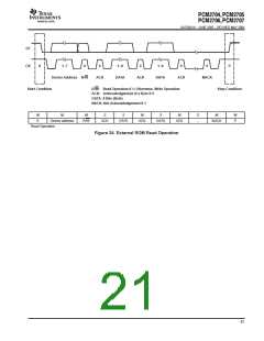
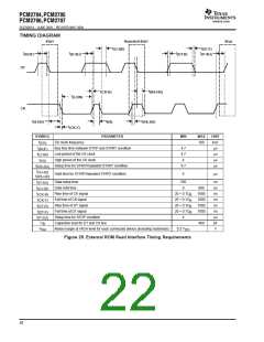
TIMING DIAGRAM
Start
Repeated Start
(D-HD)
Stop
t
t
(DT-F)
t
t
t
t
(P-SU)
(BUF)
(D-SU)
(DT-R)
DT
t
t
(RS-HD)
(CK-R)
t
(LOW)
CK
t
t
t
(RS-SU)
(S-HD)
(HI)
t
(CK-F)
SYMBOL
PARAMETER
MIN
MAX
UNIT
kHz
µs
f
CK clock frequency
100
(CK)
t
Bus free time between STOP and START condition
Low period of the CK clock
4.7
4.7
4
(BUF)
t
µs
(LOW)
t
High period of the CK clock
µs
(HI)
t
Setup time for START/repeated START condition
4.7
µs
(RS-SU)
t
(S-HD)
Hold time for START/repeated START condition
4
µs
t
(RS-HD)
t
Data setup time
250
0
ns
ns
ns
ns
ns
ns
µs
pF
V
(D-SU)
t
Data hold time
900
(D-HD)
t
Rise time of CK signal
Fall time of CK signal
Rise time of DT signal
Fall time of DT signal
Setup time for STOP condition
Capacitive load for DT and CK line
20 + 0.1C
20 + 0.1C
20 + 0.1C
20 + 0.1C
4
1000
1000
1000
1000
(CK-R)
B
B
B
B
t
t
(CK-F)
(DT-R)
t
(DT-F)
t
(P-SU)
C
B
400
V
NH
Noise margin at HIGH level for each connected device (including hysteresis)
0.2 V
DD
Figure 25. External ROM Read Interface Timing Requirements
22

 TI [ TEXAS INSTRUMENTS ]