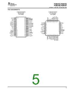
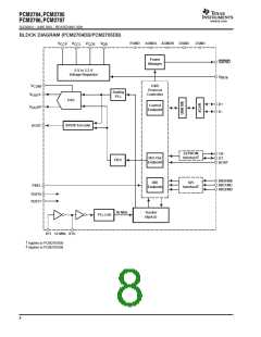
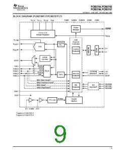
ꢀ ꢁꢂ ꢃ ꢄ ꢅ ꢆꢇ ꢀꢁ ꢂ ꢃ ꢄ ꢅ ꢈ
ꢂ
ꢀ
ꢁ
ꢂ
ꢃ
ꢄ
ꢅ
ꢉ
ꢇ
ꢀ
ꢁ
ꢃ
ꢄ
ꢅ
ꢄ
www.ti.com
SLES081A − JUNE 2003 – REVISED MAY 2004
This integrated circuit can be damaged by ESD. Texas Instruments recommends that all integrated circuits be handled with appropriate
precautions. Failure to observe proper handling and installation procedures can cause damage.
ESD damage can range from subtle performance degradation to complete device failure. Precision integrated circuits may be more susceptible to
damage because very small parametric changes could cause the device not to meet its published specifications.
(1)
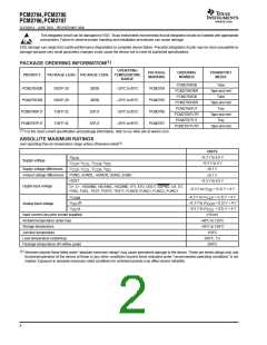
PACKAGE ORDERING INFORMATION
OPERATING
TEMPERATURE
RANGE
PACKAGE
MARKING
ORDERING
NUMBER
TRANSPORT
MEDIA
PRODUCT
PACKAGE-LEAD PACKAGE CODE
PCM2704DB
PCM2704DBR
PCM2705DB
Tube
Tape and reel
Tube
PCM2704DB
PCM2705DB
PCM2706PJT
PCM2707PJT
SSOP-28
SSOP-28
TQFP-32
TQFP-32
28DB
28DB
32PJT
32PJT
–25°C to 85°C
–25°C to 85°C
–25°C to 85°C
–25°C to 85°C
PCM2704
PCM2705
PCM2706
PCM2707
PCM2705DBR
PCM2706PJT
PCM2706PJTR
PCM2707PJT
PCM2707PJTR
Tape and reel
Tray
Tape and reel
Tray
Tape and reel
(1)
For the most current specification and package information, refer to our Web site at www.ti.com.
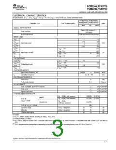
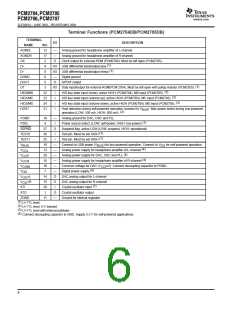
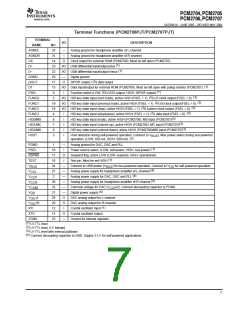
ABSOLUTE MAXIMUM RATINGS
over operating free-air temperature range unless otherwise noted
(1)
UNITS
V
V
V
–0.3 V to 6.5 V
–0.3 V to 4 V
±0.1 V
BUS
Supply voltage
, V
, V
, V
CCP CCL CCR DD
, V , V , V
Supply voltage differences
Ground voltage differences
CCP CCL CCR DD
PGND, AGNDL, AGNDR, DGND, ZGND
HOST
±0.1 V
–0.3 V to 6.5 V
Digital input voltage
Analog input voltage
D+, D–, HID0/MS, HID1/MC, HID2/MD, XTI, XTO, DOUT, SSPND, CK, DT,
PSEL, FSEL, TEST, TEST0, TEST1, FUNC0, FUNC1, FUNC2, FUNC3
–0.3 V to (V
+ 0.3) V < 4 V
DD
V
V
V
–0.3 V to (V
+ 0.3) V < 4 V
+ 0.3) V < 4 V
+ 0.3) V < 4 V
COM
CCP
R
OUT
–0.3 V to (V
CCR
CCL
L
OUT
–0.3 V to (V
Input current (any pins except supplies)
Ambient temperature under bias
Storage temperature
±10 mA
–40°C to 125°C
–55°C to 150°C
150°C
Junction temperature
Lead temperature (soldering)
Package temperature (IR reflow, peak)
260°C, 5 s
260°C
(1)
Stresses beyond those listed under “absolute maximum ratings” may cause permanent damage to the device. These are stress ratings only, and
functional operation of the device at these or any other conditions beyond those indicated under “recommended operating conditions” is not
implied. Exposure to absolute-maximum-rated conditions for extended periods may affect device reliability.
2

 TI [ TEXAS INSTRUMENTS ]