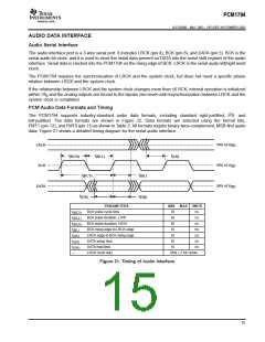
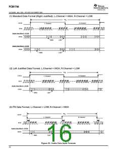
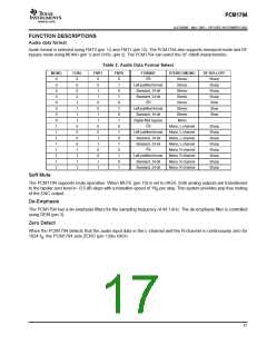
ꢀ ꢁꢂ ꢃ ꢄꢅ ꢆ
www.ti.com
SLES080B – MAY 2003 – REVISED NOVEMBER 2003
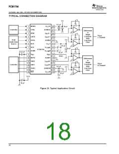
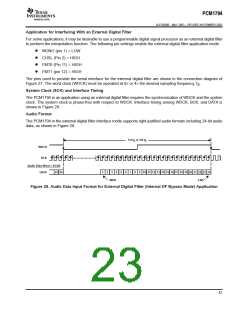
APPLICATION INFORMATION
APPLICATION CIRCUIT
The design of the application circuit is very important in order to actually realize the high S/N ratio of which the
PCM1794 is capable. This is because noise and distortion that are generated in an application circuit are not
negligible.
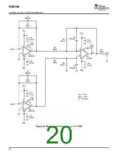
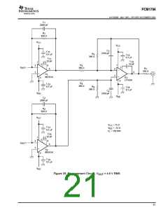
In the circuit of Figure 24, the output level is 2 V RMS, and 127 dB S/N is achieved. The circuit of Figure 25 can realize
the highest performance. In this case the output level is set to 4.5 V RMS and 129 dB S/N is achieved (stereo mode).
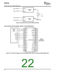
In monaural mode, if the output of the L-channel and R-channel is used as a balanced output, 132 dB S/N is achieved
(see Figure 26).
I/V Section
The current of the PCM1794 on each of the output pins (I
L+, I
L–, I
R+, I
R–) is 7.8 mA p-p at 0 dB (full
OUT
OUT
OUT
OUT
scale). The voltage output level of the I/V converter (Vi) is given by following equation:
Vi = 7.8 mA p–p × R (R : feedback resistance of I/V converter)
f
f
An NE5534 op amp is recommended for the I/V circuit to obtain the specified performance. Dynamic performance
such as the gain bandwidth, settling time, and slew rate of the op amp affects the audio dynamic performance of the
I/V section.
Differential Section
The PCM1794 voltage outputs are followed by differential amplifier stages, which sum the differential signals for each
channel, creating a single-ended I/V op-amp output. In addition, the differential amplifiers provide a low-pass filter
function.
The op amp recommended for the differential circuit is the Linear Technology LT1028, because its input noise is low.
19

 TI [ TEXAS INSTRUMENTS ]