ꢀ ꢁꢂ ꢃ ꢄꢅ ꢆ
www.ti.com
SLES080B – MAY 2003 – REVISED NOVEMBER 2003
AUDIO DATA INTERFACE
Audio Serial Interface
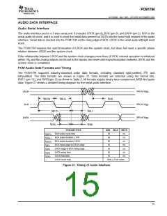
The audio interface port is a 3-wire serial port. It includes LRCK (pin 4), BCK (pin 6), and DATA (pin 5). BCK is the
serial audio bit clock, and it is used to clock the serial data present on DATA into the serial shift register of the audio
interface. Serial data is clocked into the PCM1794 on the rising edge of BCK. LRCK is the serial audio left/right word
clock.
The PCM1794 requires the synchronization of LRCK and the system clock, but does not need a specific phase
relation between LRCK and the system clock.
If the relationship between LRCK and the system clock changes more than 6 BCK, internal operation is initialized
within 1/f and the analog outputs are forced to the bipolar zero level until resynchronization between LRCK and the
S
system clock is completed.
PCM Audio Data Formats and Timing
2
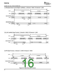
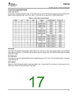
The PCM1794 supports industry-standard audio data formats, including standard right-justified, I S, and
left-justified. The data formats are shown in Figure 22. Data formats are selected using the format bits,
FMT1 (pin 12), and FMT0 (pin 11) as shown in Table 2. All formats require binary twos-complement, MSB-first audio
data. Figure 21 shows a detailed timing diagram for the serial audio interface.
50% of V
50% of V
50% of V
LRCK
DD
DD
DD
t
t
(BCL)
t
(BCH)
(LB)
BCK
t
t
(BCY)
(BL)
DATA
t
t
(DS)
(DH)
PARAMETERS
MIN MAX UNITS
t
t
t
t
t
t
t
BCK pulse cycle time
BCK pulse duration, LOW
BCK pulse duration, HIGH
BCK rising edge to LRCK edge
LRCK edge to BCK rising edge
DATA setup time
70
30
30
10
10
10
10
ns
ns
ns
ns
ns
ns
ns
(BCY)
(BCL)
(BCH)
(BL)
(LB)
(DS)
DATA hold time
(DH)
—
LRCK clock duty
50% 2 bit clocks
Figure 21. Timing of Audio Interface
15

 TI [ TEXAS INSTRUMENTS ]