PCM1794A
www.ti.com.cn
ZHCSEE9B –AUGUST 2004–REVISED DECEMBER 2015
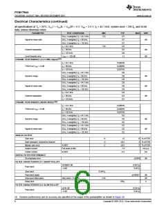
Electrical Characteristics (continued)
all specifications at TA = 25°C, VCC1 = VCC2L = VCC2R = 5 V, VDD = 3.3 V, fS = 44.1 kHz, system clock = 256 fS, and 24-bit
data, unless otherwise noted
PARAMETER
TEST CONDITIONS
MIN
TYP
MAX
UNIT
Stop band
0.732 fS
Pass-band ripple
Stop-band attenuation
±0.001
dB
dB
s
Stop band = 0.732 fS
–100
Delay time
18 / fS
POWER SUPPLY REQUIREMENTS
fS = 44.1 kHz
fS = 96 kHz
fS = 192 kHz
fS = 44.1 kHz
fS = 96 kHz
fS = 192 kHz
fS = 44.1 kHz
fS = 96 kHz
fS = 192 kHz
12
23
15
40
IDD
Digital supply current(4)
Analog supply current(4)
Power dissipation(4)
mA
mA
mW
45
33
ICC
35
37
205
250
335
250
(4) Input is BPZ data.
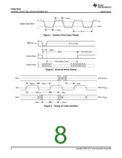
6.6 Timing Requirements
MIN
MAX
UNIT
SYSTEM CLOCK INPUT TIMING (see Figure 1)
t(SCY)
System-clock pulse-cycle time
13
0.4 × t(SCY)
0.4 × t(SCY)
ns
ns
ns
t(SCKH)
t(SCKL)
System-clock pulse duration, HIGH
System-clock pulse duration, LOW
EXTERNAL RESET TIMING (see Figure 2)
t(RST) Reset pulse duration, LOW
AUDIO INTERFACE TIMING (see Figure 3)
20
ns
t(BCY)
t(BCL)
t(BCH)
t(BL)
BCK pulse-cycle time
BCK pulse duration, LOW
BCK pulse duration, HIGH
BCK rising edge to LRCK edge
LRCK edge to BCK rising edge
DATA setup time
70
30
30
10
10
10
10
ns
ns
ns
ns
ns
ns
ns
t(LB)
t(DS)
t(DH)
DATA hold time
LRCK clock duty
50% ± 2-bit clocks
Copyright © 2004–2015, Texas Instruments Incorporated
7

 TI [ TEXAS INSTRUMENTS ]