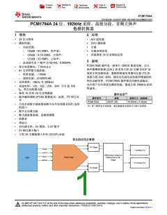
PCM1794A
ZHCSEE9B –AUGUST 2004–REVISED DECEMBER 2015
www.ti.com.cn
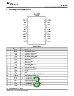
Pin Functions (continued)
PIN
I/O
DESCRIPTION
NO.
23
24
25
26
27
28
NAME
VCC
1
—
—
O
Analog power supply, 5 V
AGND2
IOUTL+
Analog ground (internal bias)
L-channel analog current output +
L-channel analog current output –
Analog ground (L-channel DAC)
Analog power supply (L-channel DAC), 5 V
IOUTL–
O
AGND3L
VCC2L
—
—
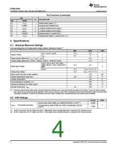
6 Specifications
6.1 Absolute Maximum Ratings
over operating free-air temperature range (unless otherwise noted)
(1)
MIN
–0.3
–0.3
MAX
6.5
UNIT
VCC1, VCC2L, VCC2R
Supply Voltage
V
VDD
4
Supply voltage differences: VCC1, VCC2L, VCC2R
±0.1
±0.1
V
V
Ground voltage differences: AGND1, AGND2, AGND3L, AGND3R, DGND
LRCK, DATA, BCK, SCK, FMT1,
FMT0, MONO, CHSL, DEM, MUTE,
RST
–0.3
6.5
Digital input voltage
V
ZERO
–0.3
–0.3
(VDD + 0.3 V) < 4
Analog input voltage
(VCC + 0.3 V) < 6.5
V
mA
°C
°C
°C
°C
°C
Input current (any pins except supplies)
Ambient temperature under bias
Junction temperature
±10
125
150
260
250
150
–40
Lead temperature (soldering, 5 s)
Package temperature (IR reflow, peak)
Storage temperature, Tstg
–55
(1) Stresses beyond those listed under Absolute Maximum Ratings may cause permanent damage to the device. These are stress ratings
only, which do not imply functional operation of the device at these or any other conditions beyond those indicated under Recommended
Operating Conditions. Exposure to absolute-maximum-rated conditions for extended periods may affect device reliability.
6.2 ESD Ratings
VALUE
UNIT
Human-body model (HBM), per ANSI/ESDA/JEDEC JS-001(1)
±2500
V(ESD)
Electrostatic discharge
V
Charged-device model (CDM), per JEDEC specification JESD22-
C101(2)
±1500
(1) JEDEC document JEP155 states that 500-V HBM allows safe manufacturing with a standard ESD control process.
(2) JEDEC document JEP157 states that 250-V CDM allows safe manufacturing with a standard ESD control process.
4
Copyright © 2004–2015, Texas Instruments Incorporated

 TI [ TEXAS INSTRUMENTS ]