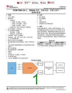
PCM1794A
www.ti.com.cn
ZHCSEE9B –AUGUST 2004–REVISED DECEMBER 2015
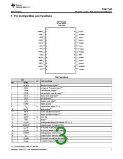
5 Pin Configuration and Functions
DB Package
28-Pin SSOP
Top View
MONO
CHSL
DEM
1
28
27
26
25
24
23
22
21
20
19
18
17
16
15
V
CC2L
2
AGND3L
3
I
I
OUTL–
LRCK
DATA
BCK
4
OUTL+
5
AGND2
6
V
V
V
CC1
SCK
7
COML
COMR
REF
DGND
8
V
9
I
DD
MUTE
FMT0
FMT1
ZERO
RST
10
11
12
13
14
AGND1
I
I
OUTR–
OUTR+
AGND3R
V
CC2R
Pin Functions
PIN
NAME
I/O
DESCRIPTION
NO.
1
MONO
CHSL
DEM
I
I
Monaural mode enable(1)
L-channel, R-channel select(1)
De-emphasis enable(1)
2
3
I
4
LRCK
DATA
BCK
I
Left and right clock (fS) input(1)
Serial audio data input(1)
Bit clock input(1)
5
I
6
I
7
SCK
I
System clock input(1)
8
DGND
VDD
—
—
I
Digital ground
9
Digital power supply, 3.3 V
Mute control(1)
Audio data format select(1)
Audio data format select(1)
Zero flag
10
11
12
13
14
15
16
17
18
19
20
21
22
MUTE
FMT0
FMT1
ZERO
RST
I
I
O
I
Reset(1)
VCC2R
AGND3R
IOUTR+
IOUTR–
AGND1
IREF
—
—
O
O
—
—
—
—
Analog power supply (R-channel DAC), 5 V
Analog ground (R-channel DAC)
R-channel analog current output +
R-channel analog current output –
Analog ground (internal bias)
Output current reference bias pin
R-channel internal bias decoupling pin
L-channel internal bias decoupling pin
VCOMR
VCOM
L
(1) Schmitt-trigger input, 5-V tolerant.
Copyright © 2004–2015, Texas Instruments Incorporated
3

 TI [ TEXAS INSTRUMENTS ]