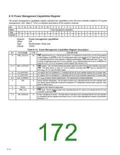
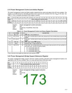
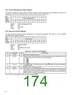
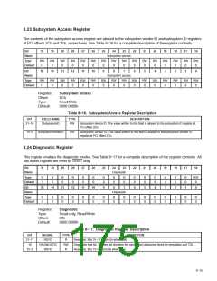
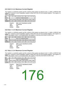
8.25 Slot 0 3.3-V Maximum Current Register
This register is a read/write register and the contents of this register are aliased to the 3_3_MAX_CURRENT field
in the slot 0 maximum current capabilities register at offset 48h in the SD host standard registers. This register is a
GRST only register.
Bit
7
6
5
4
3
2
1
0
Name
Type
Default
Slot 0 3.3-V maximum current
RW
0
RW
0
RW
0
RW
0
RW
0
RW
0
RW
0
RW
0
Register:
Type:
Offset:
Default:
Slot 3.3-V maximum current
Read/Write
94h
0000h
8.26 Slot 1 3.3-V Maximum Current Register
This register is a read/write register and the contents of this register are aliased to the 3_3_MAX_CURRENT field
in the slot 1 maximum current capabilities register at offset 48h in the SD host standard registers. This register is a
GRST only register. If slot 1 is not implemented, this register is read-only and returns 0s when read.
Bit
7
6
5
4
3
2
1
0
Name
Type
Default
Slot 1 3.3-V maximum current
RW
0
RW
0
RW
0
RW
0
RW
0
RW
0
RW
0
RW
0
Register:
Type:
Offset:
Default:
Slot 1 3.3-V maximum current
Read/Write
98h
0000h
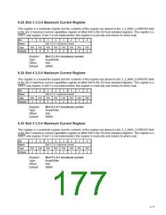
8.27 Slot 2 3.3-V Maximum Current Register
This register is a read/write register and the contents of this register are aliased to the 3_3_MAX_CURRENT field
in the slot 2 maximum current capabilities register at offset 48h in the SD host standard registers. This register is a
GRST only register. If slot 2 is not implemented, this register is read-only and returns 0s when read.
Bit
7
6
5
4
3
2
1
0
Name
Type
Default
Slot 2 3.3-V maximum current
RW
0
RW
0
RW
0
RW
0
RW
0
RW
0
RW
0
RW
0
Register:
Type:
Offset:
Default:
Slot 2 3.3-V maximum current
Read/Write
9Ch
0000h
8−16

 TI [ TEXAS INSTRUMENTS ]