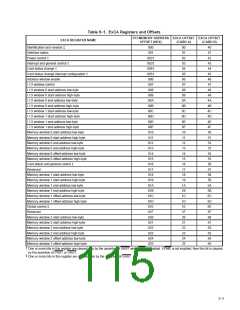
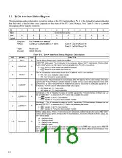
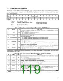
5.3 ExCA Power Control Register
This register provides PC Card power control. Bit 7 of this register enables the 16-bit outputs on the socket interface,
and can be used for power management in 16-bit PC Card applications. See Table 5−5 for a complete description
of the register contents.
Bit
7
6
5
4
3
2
1
0
Name
Type
Default
ExCA power control
RW
0
R
0
R
0
RW
0
RW
0
R
0
RW
0
RW
0
Register:
Offset:
ExCA power control
CardBus Socket Address + 802h:
Card A ExCA Offset 02h
Card B ExCA Offset 42h
Type:
Default:
Read-only, Read/Write
00h
Table 5−4. ExCA Power Control Register Description—82365SL Support
BIT
SIGNAL
TYPE
FUNCTION
Card output enable. Bit 7 controls the state of all of the 16-bit outputs on the PCI6x21/PCI6x11 controller.
This bit is encoded as:
7
COE
RW
0 = 16-bit PC Card outputs disabled (default)
1 = 16-bit PC Card outputs enabled
6
RSVD
R
Reserved. Bit 6 returns 0 when read.
Auto power switch enable.
5 †
AUTOPWRSWEN
RW
0 = Automatic socket power switching based on card detects is disabled.
1 = Automatic socket power switching based on card detects is enabled.
PC Card power enable.
0 = V
1 = V
= No connection
CC
CC
4
CAPWREN
RSVD
RW
R
is enabled and controlled by bit 2 (EXCAPOWER) of the system control register
(PCI offset 80h, see Section 4.29).
3−2
1−0
Reserved. Bits 3 and 2 return 0s when read.
PC Card V
PP
controller ignores this field unless V
00 = No connection (default)
power control. Bits 1 and 0 are used to request changes to card V . The PCI6x21/PCI6x11
PP
to the socket is enabled. This field is encoded as:
CC
EXCAVPP
RW
10 = 12 V
01 = V
CC
11 = Reserved
†
One or more bits in this register are cleared only by the assertion of GRST when PME is enabled. If PME is not enabled, then this bit is cleared
by the assertion of PRST or GRST.
Table 5−5. ExCA Power Control Register Description—82365SL-DF Support
BIT
SIGNAL
TYPE
FUNCTION
Card output enable. This bit controls the state of all of the 16-bit outputs on the PCI6x21/PCI6x11 controller.
This bit is encoded as:
7 †
COE
RW
0 = 16-bit PC Card outputs are disabled (default).
1 = 16-bit PC Card outputs are enabled.
6−5
4−3 †
2
RSVD
EXCAVCC
RSVD
R
RW
R
Reserved. These bits return 0s when read. Writes have no effect.
V
. These bits are used to request changes to card V . This field is encoded as:
CC
CC
00 = 0 V (default)
01 = 0 V reserved
10 = 5 V
11 = 3.3 V
This bit returns 0 when read. A write has no effect.
V
. These bits are used to request changes to card V . The PCI6x21/PCI6x11 controller ignores this
PP
PP
field unless V
to the socket is enabled (i.e., 5 Vdc or 3.3 Vdc). This field is encoded as:
CC
1−0 †
EXCAVPP
RW
00 = 0 V (default)
01 = V
10 = 12 V
11 = 0 V reserved
CC
†
This bit is cleared only by the assertion of GRST when PME is enabled. If PME is not enabled, then this bit is cleared by the assertion of PRST
or GRST.
5−7

 TI [ TEXAS INSTRUMENTS ]